LTC1698
W U U
APPLICATIO S I FOR ATIO
U
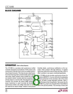
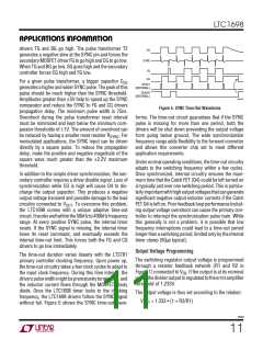
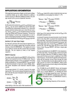
drivers TG and BG go high. The pulse transformer T2
generates a negative slew at the SYNC pin and forces the
secondary MOSFET driver FG to go high and CG to go low.
When TG and BG go low, SG goes high and the secondary
controller forces CG high and FG low.
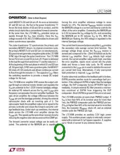
SG
SYNC
FG
CG
For a given pulse transformer, a bigger capacitor CSG
generates a higher and wider SYNC pulse. The peak of this
pulse should be much higher than the SYNC threshold.
Amplitudes greater than ±5V help to speed up the SYNC
comparator and reduce the SYNC to FG and CG drivers
propagation delay. The minimum pulse width is 75ns.
Overshoot during the pulse transformer reset interval
must be minimized and kept below the minimum com-
parator thresholds of ±1V. The amount of overshoot can
be reduced by having a smaller reset resistor RSYNC. For
nonisolated applications, the SYNC input can be driven
directly by a square pulse. To reduce the propagation
delay, make the positive and negative magnitude of the
square wave much greater than the ±2.2V maximum
threshold.
RESET
(INTERNAL)
DISDRI
(INTERNAL)
1698 F05
Figure 5. SYNC Time-Out Waveforms
forms. The time-out circuit guarantees that if the SYNC
pulse is missing for more than one period, both the
drivers will be shut down preventing the output voltage
from going below ground. The wide synchronization
frequency range adds flexibility to the forward converter
and allows this converter chip set to meet different
application requirements.
Under normal operating conditions, the time-out circuitry
adapts to the switching frequency within a few cycles.
Once synchronized, internal circuitry ensures the maxi-
mum time that the Catch FET (Q4) could be left turned on
is typically just over one switching period. This is particu-
larlyimportantwithhighoutputvoltagesthatcangenerate
significant negative output inductor currents if the Catch
FET Q4 is left on. Poor feedback loop performance includ-
ing output voltage overshoot can cause the primary con-
troller to interrupt the synchronization pulse train. While
this generally is not a problem, it is possible that low
frequency interruptions could lead to a time-out period
longer than a switching period, limited only by the internal
timer clamp (50µs typical).
In addition to the simple driver synchronization, the sec-
ondary controller requires a driver disable signal. Loss of
synchronization while CG is high will cause Q4 to dis-
charge the output capacitor. This produces a negative
output voltage transient and possible damage to the load
circuitry connected to VOUT. To overcome this problem,
the LTC1698 comes with a unique adaptive time-out
circuit. Itworkswellwithinthe50kHzto400kHzfrequency
range. At every positive SYNC pulse, the internal timer
resets. If the SYNC signal is missing, the internal timer
loses its reset command, and eventually exceeds the
internal time-out limit. This forces both the FG and CG
drivers to go low immediately.
Output Voltage Programming
The time-out duration varies linearly with the LT3781
primary controller clocking frequency. Upon power up,
the time-out circuitry takes a few clock cycles to adapt to
the input clock frequency. During this time interval, the
driverspulsewidthmightbeprematurelyterminated, and
the inductor current flows through the MOSFETs body
diode. Once the LTC1698 timer locks to the clocking
frequency, the LTC1698 drivers follow the SYNC signal
without fail. Figure 5 shows the SYNC time-out wave-
The switching regulator output voltage is programmed
through a resistor feedback network (R1 and R2 in
Figure 1) connected to VFB. If the output is at its nominal
value,thedivideroutputisregulatedtotheerroramplifier
threshold of 1.233V.
The output voltage is thus set according to the relation:
VOUT = 1.233 • (1 + R2/R1)
1698f
11

 Linear [ Linear ]