LTC1698
U
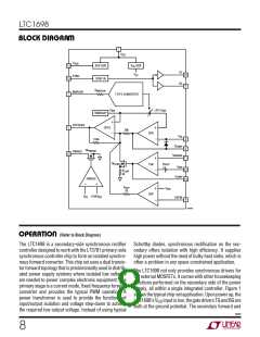
OPERATIO
(Refer to Block Diagram)
catch MOSFETs Q3 and Q4 are off. As soon as transistors
Q1 and Q2 turn on, the flux in the power transformer T1
forces the body diodes of Q3 and Q4 to conduct, and the
whole circuit starts like a conventional forward converter.
At the same time, the LTC1698 VDD potential ramps up
quickly through the VDD bias circuitry. Once the VDD
voltageexceeds4.0V, theLTC1698enablesitsdriversand
enters synchronous operation.
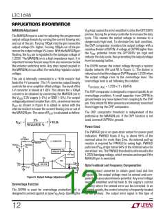
forcing the error amplifier reference voltage to move
linearly by ±5%. The internal RMARGIN resistor converts
the MARGIN voltage to a current and linearly controls the
offset of the error amplifier. Connecting the MARGIN pin
to 3.3V increases the VFB voltage by 5%, and connecting
the MARGIN pin to 0V reduces VFB by 5%. With the
MARGIN pin floating, the VFB voltage is regulated to the
internal bandgap voltage.
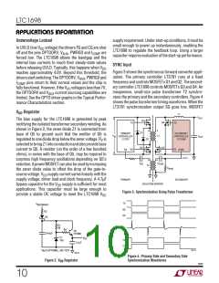
The pulse transformer T2 synchronizes the primary and
secondary MOSFET drivers. In a typical conversion cycle,
the primary MOSFETs Q1 and Q2 turn on simultaneously.
SGgoeslowandgeneratesanegativespikeattheLTC1698
SYNC input through the pulse transformer. The LTC1698
forces FG to turn on and CG to turn off. Power is delivered
totheloadthroughthetransformerT1andtheinductorL1.
At the beginning of the next phase in which Q1 and Q2 turn
off,SGgoeshigh,SYNCseesapositivespike,theMOSFET
Q3 shuts off, Q4 conducts and allows continuous current
to flow through the inductor L1. The capacitor COUT filters
the switching waveform to provide a steady DC output
voltage for the load.
ThecurrentlimittransconductanceamplifierILIM provides
the secondary side average current limit function. The
average voltage drops across the RSECSEN resistor is
sensed and compared to the –25mV threshold set by the
internal ILIM amplifier. Once ILIM detects high output
current, the current amplifier output pulls high, overrides
the error amplifier, injects more current into the photo
diode and forces a lower duty cycle. An RC network
connected to the ICOMP pin is used to stabilize the second-
ary current limit loop. Alternatively, if only overcurrent
fault protection is required, ICOMP can float.
If under abnormal conditions the feedback path is broken,
OVPIN provides another route for overvoltage fault pro-
tection. If the voltage at OVPIN is higher than the bandgap
voltage, the OVP comparator forces OPTODRV high im-
mediately. A simple external RC filter prevents a momen-
tary overshoot at OVPIN from triggering the OVP
comparator. Short OVPIN to ground if this pin is not used.
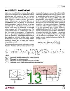
The LTC1698 error amplifier ERR senses the output volt-
age through an external resistor divider and regulates the
VFB pin potential to the 1.233V internal bandgap voltage.
An external RC network across the VFB and VCOMP pins
frequency compensates the error amplifier feedback. The
opto driver amplifies the voltage difference between the
VCOMP pin and the bandgap potential, driving the external
optocoupler diode with an inverting gain of 5. The
optocoupler feeds the amplified output error signal to the
primary controller and closes the forward converter volt-
age feedback loop. Under start-up conditions, the internal
diode across the LTC1698 error amplifier clamps the
VCOMP pin.Thisspeedsuptheoptodriverrecoverytimeby
reducingthenegativeslewrateexcursionattheCOMPpin.
The LTC1698 provides an open-drain PWRGD output. If
VFB is less than 94% of its nominal value for more than
1ms, the PWRGD comparator pulls the PWRGD pin low.
IfVFB ishigherthan94%ofitsnominalvalueformorethan
2ms, the transistor MPWRGD shuts off, and an external
resistor pulls the PWRGD pin high.
The LTC1698 provides an auxiliary 3.3V logic power
supply. This auxiliary power supply is externally compen-
sated with a minimum 0.1µF bypass capacitor. It supplies
up to 10mA of current to any external devices.
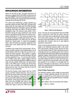
The forward converter output voltage can be easily ad-
justed. The potential at the MARGIN pin is capable of
1698f
9

 Linear [ Linear ]