LTC1698
W U U
U
APPLICATIO S I FOR ATIO
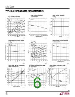
Undervoltage Lockout
supply requirement. Under start-up conditions, it must be
small enough to power up instantaneously, enabling the
LTC1698 to regulate the feedback loop. Using a larger
capacitor requires evaluation of the start-up performance.
In UVLO (low VDD voltage) the drivers FG and CG are shut
off and the pins OPTODRV, VAUX, PWRGD and ICOMP are
forced low. The LTC1698 allows the bandgap and the
internal bias currents to reach their steady-state values
before releasing UVLO. Typically, this happens when VDD
reaches approximately 4.0V. Beyond this threshold, the
driversstartswitching. TheOPTODRV, VAUX, PWRGDand
ICOMP pins return to their normal values and the chip is
fullyfunctional.However,iftheVDD voltageislessthan7V,
the OPTODRV and VAUX current sourcing capabilities are
limited. See the OPTO driver graphs in the Typical Perfor-
mance Characteristics section.
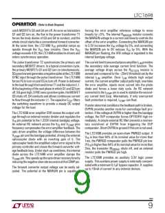
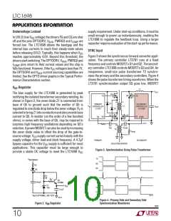
SYNC Input
Figure 3 shows the synchronous forward converter appli-
cation. The primary controller LT3781 runs at a fixed
frequencyandcontrolsMOSFETsQ1andQ2. Thesecond-
ary controller LTC1698 controls MOSFETs Q3 and Q4. An
inexpensive, small-size pulse transformer T2 synchro-
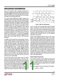
nizes the primary and the secondary controllers. Figure 4
showsthepulsetransformertimingwaveforms. Whenthe
LT3781 synchronization output SG goes low, MOSFET
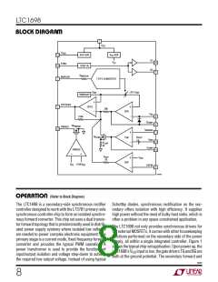
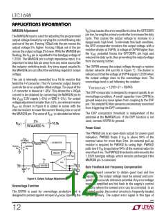
VDD Regulator
L1
V
OUT
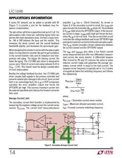
The bias supply for the LTC1698 is generated by peak
rectifying the isolated transformer secondary winding. As
shown in Figure 2, the zener diode Z1 is connected from
base of Q5 to ground such that the emitter of Q5 is
regulated to one diode drop below the zener voltage. RZ is
selectedtobringZ1intoconductionandalsoprovidebase
current to Q5. A resistor (on the order of a few hundred
ohms), in series with the base of Q5, may be required to
surpress high frequency oscillations depending on Q5’s
selection.ApowerMOSFETcanalsobeusedbyincreasing
the zener diode value to offset the drop of the gate-to-
source voltage. VDD supply current varies linearly with the
supply voltage, driver load and clock frequency. A 4.7µF
bypass capacitor for the VDD supply is sufficient for most
applications. This capacitor must be large enough to
provide a stable DC voltage to meet the LTC1698 VDD
Q1
Q4
TG
CG
•
•
D1
PRIMARY
CONTROLLER
LT3781
SECONDARY
CONTROLLER
LTC1698
V
T1
C
OUT
IN
D2
Q2
Q3
BG
SG
FG
SYNC
1698 F03
•
•
C
C
SYNC
SG
T2
R
SYNC
PRIMARY
SECONDARY
ISOLATION BARRIER
Figure 3. Synchronization Using Pulse Transformer
TG
V
SECONDARY
BG
SG
1Ω
D3
R
Z
SYNC
2k
R *
B
Q5
FZT690
0.47µF
Z1
10V
V
DD
FG
4.7µF
CG
1698 F04
*R IS OPTIONAL, SEE TEXT
B
1698 F02
Figure 4. Primary Side and Secondary Side
Synchronization Waveforms
Figure 2. VDD Regulator
1698f
10

 Linear [ Linear ]