LTC1698
W U U
U
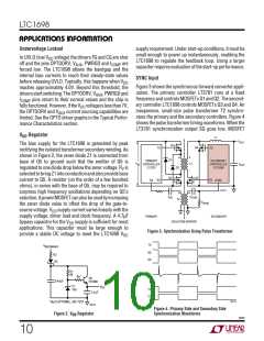
APPLICATIO S I FOR ATIO
A series RC network can be added in parallel with R2
(Figure 7) to provide a zero for the feedback loop fre-
quency compensation.
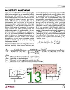
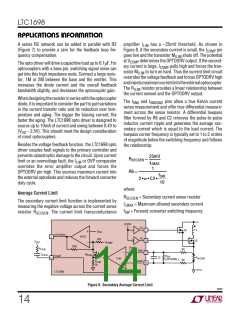
amplifier ILIM has a –25mV threshold. As shown in
Figure 8, if the secondary current is small, the ICOMP pin
goes low and the transistor MILIM shuts off. The potential
at VCOMP determines the OPTODRV output. If the second-
ary current is large, ICOMP pulls high and forces the tran-
sistor MILIM to turn on hard. Thus the current limit circuit
overrides the voltage feedback and forces OPTODRV high
andinjectsmaximumcurrentintotheexternaloptocoupler.
The RILIM resistor provides a linear relationship between
the current sensed and the OPTODRV output.
The opto driver will drive a capacitive load up to 0.1µF. For
optocouplers with a base pin, switching signal noise can
get into this high impedance node. Connect a large resis-
tor, 1M or 2M between the base and the emitter. This
increases the diode current and the overall feedback
bandwidth slightly, and decreases the optocoupler gain.
Whendesigningtheresistorinserieswiththeoptocoupler
diode, it is important to consider the part to part variations
in the current transfer ratio and its reduction over tem-
perature and aging. The bigger the biasing current, the
faster the aging. The LTC1698 opto driver is designed to
source up to 10mA of current and swing between 0.4V to
(VDD – 2.5V). This should meet the design consideration
of most optocouplers.
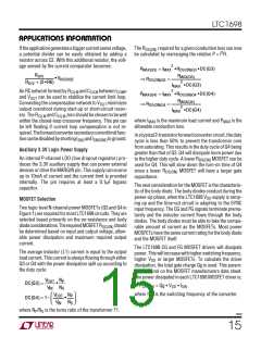
The ISNS and ISNSGND pins allow a true Kelvin current
sense measurement and offer true differential measure-
ment across the sense resistor. A differential lowpass
filter formed by R6 and C2 removes the pulse-to-pulse
inductor current ripple and generates the average sec-
ondary current which is equal to the load current. The
lowpass corner frequency is typically set to 1 to 2 orders
of magnitude below the switching frequency and follows
the relationship:
Besides the voltage feedback function, the LTC1698 opto
driver couples fault signals to the primary controller and
prevents catastrophic damage to the circuit. Upon current
limit or an overvoltage fault, the ILIM or OVP comparator
overrides the error amplifier output and forces the
OPTODRV pin high. This sources maximum current into
the external optodiode and reduces the forward converter
duty cycle.
25mV
ILMAX
1
RSECSEN
=
R6 =
fSW
10
2• π •C2•
where:
Average Current Limit
RSECSEN = Secondary current sense resistor
ILMAX = Maximum allowed secondary current
fSW = Forward converter switching frequency
The secondary current limit function is implemented by
measuring the negative voltage across the current sense
resistor RSECSEN. The current limit transconductance
DRIVE
CG
2
Q4
T1
V
REF
+
OPTODRV
5
OPTO
FG
20k
16
Q3
V
OUT
V
COMP
–
100k
25mV
R
CILM
R6
I
–
+
SNS
+
12
11
C
CILM
M
ILIM
I
COMP
R
DIV
(OPTIONAL)
C2
R
13
I
LIM
SECSEN
R6
I
SNSGND
R
ILIM
3k
1698 F08
LTC1698
Figure 8. Secondary Average Current Limit
1698f
14

 Linear [ Linear ]