LTC1698
W U U
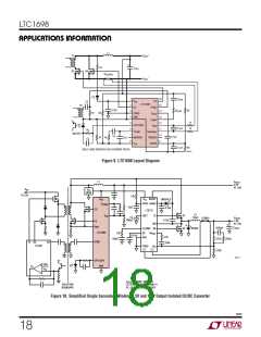
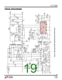
APPLICATIO S I FOR ATIO
U
Iftheapplicationgeneratesabiggercurrentsensevoltage,
a potential divider can be easily obtained by adding a
resistor across C2. With this additional resistor, the volt-
age sensed by the current comparator becomes:
The RDS(ON) required for a given conduction loss can now
be calculated by rearranging the relation P = I2R.
PMAX(Q3) = IMAX2 •RDS(ON)Q3 •DC(Q3)
RDIV
DIV + (2•R6)
PMAX(Q3)
IMAX2 •DC(Q3)
•VRSENSE
RDS(ON)Q3
=
R
PMAX(Q4) = IMAX2 •RDS(ON)Q4 •DC(Q4)
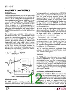
An RC network formed by RCILM and CCILM between ICOMP
and VOUT can be used to stabilize the current limit loop.
Connecting the compensation network to VOUT minimizes
output overshoot during start-up or short-circuit recov-
ery. The RCILM and CCILM zero should be chosen to be well
within the closed-loop crossover frequency. This pin can
be left floating if current loop compensation is not re-
quired.Theforwardconvertersecondarycurrentlimitfunc-
tioncanbedisabledbyshortingISNSandISNSGND toground.
PMAX(Q4)
IMAX2 •DC(Q4)
RDS(ON)Q4
=
where IMAX is the maximum load current and PMAX is the
allowable conduction loss.
Inatypical2-transistorforwardconvertercircuit,theduty
cycle is less than 50% to prevent the transformer core
from saturating. This results in the duty cycle of Q4 being
greater than that of Q3. Q4 will dissipate more power due
to the higher duty cycle. A lower RDS(ON) MOSFET can be
used for Q4. This will slow down the turn-on time of Q4
since a lower RDS(ON) MOSFET will have a larger gate
capacitance.
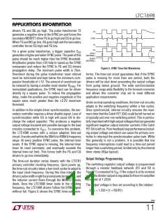
Auxiliary 3.3V Logic Power Supply
An internal P-channel LDO (low dropout regulator) pro-
duces the 3.3V auxiliary supply that can power external
devices or drive the MARGIN pin. This supply can source
up to 10mA of current and the current limit is provided
internally. The pin requires at least a 0.1µF bypass
capacitor.
The next consideration for the MOSFET is the characteris-
tic of the body diode. The body diodes conduct during the
power-up phase, when the LTC1698 VDD supply is ramp-
ing up and the time-out circuit is adapting to the SYNC
input frequency. The CG and FG signals terminate prema-
turely and the inductor current flows through the body
diodes. The body diodes must be able to take the compa-
rable amount of current as the MOSFETs. Most power
MOSFETs have the same current rating for the body diode
and the MOSFET itself.
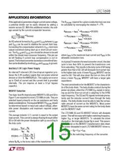
MOSFET Selection
Two logic-level N-channel power MOSFETs (Q3 and Q4 in
Figure 1) are required for most LTC1698 circuits. They are
selected based primarily on the on-resistance and body
diodeconsiderations.TherequiredMOSFETRDS(ON) should
be determined based on input and output voltage, allow-
able power dissipation and maximum required output
current.
The LTC1698 CG and FG MOSFET drivers will dissipate
power. This will increase with higher switching frequency,
higher VDD or larger MOSFETs. To calculate the driver
dissipation, the total gate charge Qg is used. This param-
eter is found on the MOSFET manufacturers data sheet.
The power dissipated in each LTC1698 MOSFET driver is:
The average inductor (L1) current is equal to the output
load current. This current is always flowing through either
Q3 or Q4 with the power dissipation split up according to
the duty cycle:
VOUT NP
DC(Q3) =
•
PDRIVER = Qg • VDD • fSW
V
NS
VOUT NP
IN
where fSW is the switching frequency of the converter.
DC(Q4) = 1–
•
V
IN
NS
where NP/NS is the turns ratio of the transformer T1.
1698f
15

 Linear [ Linear ]