LTC1698
W U U
U
APPLICATIO S I FOR ATIO
MARGIN Adjustment
VFB loop causes the error amplifier to drive the OPTODRV
pin low, forcing the primary controller to increase the duty
cycle. This causes the output voltage to increase to a
dangerously high level. To eliminate this fault condition,
the OVP comparator monitors the output voltage with a
resistive divider at OVPIN. A voltage at OVPIN higher than
the VREF potential forces the OPTODRV pin high and
reduces the duty cycle, thus preventing the output voltage
from increasing further.
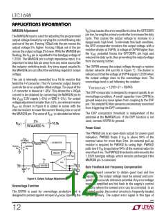
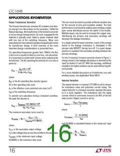
The MARGIN input is used for adjusting the programmed
output voltage linearly by varying the current flowing into
and out of the pin. Forcing 100µA into the pin moves the
output voltage 5% higher. Forcing 100µA out of the pin
moves the output voltage 5% lower. With the MARGIN pin
floating, the VFB pin is regulated to the bandgap voltage of
1.233V. The MARGIN pin is a high impedance input. It is
important to keep this pin away from any noise source like
the inductor switching node. Any stray signal coupled to
the MARGIN pin can affect the switching regulator output
voltage.
The OVPIN senses the output voltage through a resistor
divider network (R4 and R5 in Figure 1). The divider is
ratioedsuchthatthevoltageatOVPINequals1.233Vwhen
the output voltage rises to the overvoltage level. The
overvoltage level is set following the relation:
This pin is internally connected to a 16.5k resistor that
feeds the I-V converter. The I-V converter output linearly
controls the error amplifier offset voltage. The input of the
I-V converter is biased at 1.65V. This allows the ±100µA
current to be obtained by connecting the MARGIN pin to
the VAUX 3.3V supply (+5%) or GND (–5%). For output
voltageadjustmentsmallerthan±5%, anexternalresistor
REXT as shown in Figure 6 is added in series with the
internal resistor to lower the current flowing into or out of
the MARGIN pin. The value of REXT is calculated as follow:
V
OVERVOLTAGE = 1.233 • (1 + R5/R4)
The OVP comparator is designed to respond quickly to an
overvoltage condition. A small capacitor from OVPIN to
ground keeps any noise spikes from coupling to the OVP
pin. ThissimpleRCfilterpreventsamomentaryovershoot
from triggering the OVP comparator.
The OVP comparator threshold is independent of the
potential at the MARGIN pin. If the OVP function is not
used, connect OVPIN to ground.
5%
REXT
=
– 1 •16.5k
REQUIRED %
Power Good
The PWRGD pin is an open-drain output for power good
indication. PWRGD floats if VFB is above 94% of the
nominal value for more than 2ms. An external pull-up
resistor is required for PWRGD to swing high. PWRGD
pulls low if VFB drops below 94% of the nominal value for
morethan1ms.ThePWRGDthresholdisreferencedtothe
1.233V bandgap voltage, which remains unchanged if the
MARGIN pin is exercised.
R
EXT
(OPTIONAL)
R
MARGIN
7
I-V CONVERTER
MARGIN
REDUCE
INCREASE
V
V
FB
FB
V
REF
BANDGAP
±5% V
REF
+
V
DD
ERR
V
FB
V
AUX
3.3V
14
AUX GEN
8
6
–
V
AUX
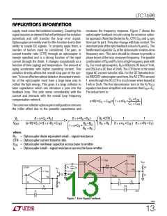
Opto Feedback and Frequency Compensation
0.1µF
V
COMP
For a forward converter to obtain good load and line
regulation, the output voltage must be sensed and com-
pared to an accurate reference potential. Any error voltage
must be amplified and fed back to the supply’s control
circuitry where the sensed error can be corrected. In an
isolated supply, the control circuitry is frequently located
on the primary. The output error signal in this type of
1698 F06
Figure 6. Output Voltage Adjustment
Overvoltage Function
The OVPIN is used for overvoltage protection and is
designed to protect against an open VFB loop. Opening the
1698f
12

 Linear [ Linear ]