LTC1698
W
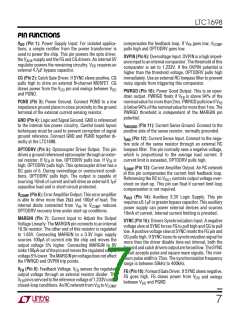
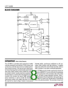
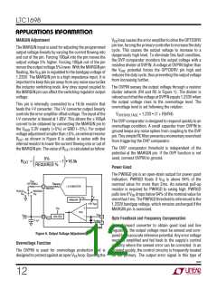
BLOCK DIAGRA
1
V
DD
V
AUX
AUX GEN
SYNC IN
V
GEN
CC
14
CC
FG
V
16
2
SYNC
15
7
CG
R
MARGIN
MARGIN
I-TO-V CONVERTER
V
REF
±5% V
REF
BANDGAP
+
–
OPTODRV
PWRGD
5
+
–
OPTO
20k
ERR
V
FB
8
6
100k
V
COMP
M
PWRGD
10
I
SNSGND
+
–
11
M
ILIM
I
LIM
25mV
+
I
SNS
12
13
R
ILIM
3k
I
COMP
PWRGD
–
+
R
OVP
3k
+
–
V
REF
OVP
V
FB
0.94V
REF
OVPIN
9
1698 BD
U
OPERATIO
(Refer to Block Diagram)
The LTC1698 is a secondary-side synchronous rectifier
controller designed to work with the LT3781 primary-side
synchronous controller chip to form an isolated synchro-
nous forward converter. This chip set uses a dual transis-
tor forward topology that is predominantly used in distrib-
uted power supply systems where isolated low voltages
are needed to power complex electronic equipment. The
primary stage is a current mode, fixed frequency forward
converter and provides the typical PWM operation. A
power transformer is used to provide the functions of
input/output isolation and voltage step-down to achieve
the required low output voltage. Instead of using typical
Schottky diodes, synchronous rectification on the sec-
ondary offers isolation with high efficiency. It supplies
high power without the need of bulky heat sinks, which is
often a problem in any space constrained application.
The LTC1698 not only provides synchronous drivers for
the external MOSFETs, it comes with other housekeeping
functions performed on the secondary side of the power
supply, all within a single integrated controller. Figure 1
showsthetypicalchip-setapplication.Uponpowerup,the
LTC1698’sVDD inputislow,thegatedriversTGandBGare
both at the ground potential. The secondary forward and
1698f
8

 Linear [ Linear ]