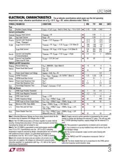
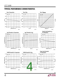
LTC1698
U
U
U
PI FU CTIO S
VDD (Pin 1): Power Supply Input. For isolated applica-
tions, a simple rectifier from the power transformer is
used to power the chip. This pin powers the opto driver,
the VAUX supply and the FG and CG drivers. An internal 5V
regulator powers the remaining circuitry. VDD requires an
external 4.7µF bypass capacitor.
compensates the feedback loop. If VFB goes low, VCOMP
pulls high and OPTODRV goes low.
OVPIN (Pin 9): Overvoltage Input. OVPIN is a high imped-
ance input to an internal comparator. The threshold of this
comparator is set to 1.233V. If the OVPIN potential is
higher than the threshold voltage, OPTODRV pulls high
immediately. Use an external RC lowpass filter to prevent
noisy signals from triggering this comparator.
CG (Pin 2): Catch Gate Driver. If SYNC slews positive, CG
pulls high to drive an external N-channel MOSFET. CG
draws power from the VDD pin and swings between VDD
and PGND.
PWRGD (Pin 10): Power Good Output. This is an open-
drain output. PWRGD floats if VFB is above 94% of the
nominal value for more than 2ms. PWRGD pulls low if VFB
is below 94% of the nominal value for more than 1ms. The
PWRGD threshold is independent of the MARGIN pin
potential.
PGND (Pin 3): Power Ground. Connect PGND to a low
impedance ground plane in close proximity to the ground
terminal of the external current sensing resistor.
GND (Pin 4): Logic and Signal Ground. GND is referenced
to the internal low power circuitry. Careful board layout
techniques must be used to prevent corruption of signal
ground reference. Connect GND and PGND together di-
rectly at the LTC1698.
I
SNSGND (Pin 11): Current Sense Ground. Connect to the
positive side of the sense resistor, normally grounded.
I
SNS (Pin 12): Current Sense Input. Connect to the nega-
tive side of the sense resistor through an external RC
lowpass filter. This pin normally sees a negative voltage,
which is proportional to the average load current. If
current limit is exceeded, OPTODRV pulls high.
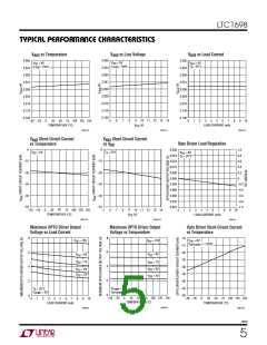
OPTODRV (Pin 5): Optocoupler Driver Output. This pin
drives a ground referenced optocoupler through an exter-
nal resistor. If VFB is low, OPTODRV pulls low. If VFB is
high, OPTODRV pulls high. This optocoupler driver has a
DC gain of 5. During overvoltage or overcurrent condi-
tions, OPTODRV pulls high. The output is capable of
sourcing 10mA of current and will drive an external 0.1µF
capacitive load and is short-circuit protected.
I
COMP (Pin 13): Current Amplifier Output. An RC network
at this pin compensates the current limit feedback loop.
Referencing the RC to VOUT controls output voltage over-
shoot on start-up. This pin can float if current limit loop
compensation is not required.
V
COMP (Pin 6):Error Amplifier Output. This error amplifier
VAUX (Pin 14): Auxiliary 3.3V Logic Supply. This pin
requiresa0.1µForgreaterbypasscapacitor.Thisauxiliary
power supply can power external devices and sources
10mA of current. Internal current limiting is provided.
is able to drive more than 2kΩ and 100pF of load. The
internal diode connected from VFB to VCOMP reduces
OPTODRV recovery time under start-up conditions.
MARGIN (Pin 7): Current Input to Adjust the Output
Voltage Linearly. The MARGIN pin connects to an internal
16.5k resistor. The other end of this resistor is regulated
to 1.65V. Connecting MARGIN to a 3.3V logic supply
sources 100µA of current into the chip and moves the
output voltage 5% higher. Connecting MARGIN to 0V
sinks 100µA out of the pin and moves the regulated output
voltage5%lower. TheMARGINpinvoltagedoesnotaffect
the PWRGD and OVPIN trip points.
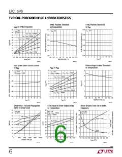
SYNC (Pin 15): Drivers Synchronization Input. A negative
voltage slew at SYNC forces FG to pull high and CG to pull
low. A positive voltage slew at SYNC resets the FG pin and
CG pulls high. If SYNC loses its synchronization signal for
more than the driver disable time-out interval, both the
forwardandcatchdriversoutputareforcedlow.TheSYNC
circuit accepts pulse and square wave signals. The mini-
mum pulse width is 75ns. The synchronization frequency
range is between 50kHz to 400kHz.
VFB (Pin 8): Feedback Voltage. VFB senses the regulated
output voltage through an external resistor divider. The
VFB pinisservoedtothereferencevoltageof1.233Vunder
closed-loopconditions. AnRCnetworkfromVFB toVCOMP
FG (Pin 16): Forward Gate Driver. If SYNC slews negative,
FG goes high. FG draws power from VDD and swings
between VDD and PGND.
1698f
7

 Linear [ Linear ]