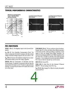
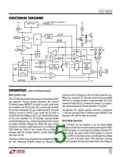
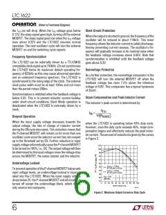
LTC1622
U
W U U
APPLICATIONS INFORMATION
In applications where the maximum duty cycle is less than
100%andtheLTC1622isincontinuousmode,theRDS(ON)
is governed by:
preferred at high switching frequencies, so design goals
canconcentrateoncopperlossandpreventingsaturation.
Ferrite core materials saturate “hard,” which means that
the inductance collapses abruptly when the peak design
current is exceeded. This results in an abrupt increase in
inductor ripple current and consequently, output voltage
ripple. Do not allow the core to saturate!
P
P
R
DS(ON)
2
OUT
1+ δp
DC I
(
)
(
)
where DC is the maximum operating duty cycle of the
LTC1622.
Molypermalloy (from Magnetics, Inc.) is a very good, low
losscorematerialfortoroids,butitismoreexpensivethan
ferrite. A reasonable compromise from the same manu-
facturer is Kool Mu. Toroids are very space efficient,
especially when you can use several layers of wire.
Because they generally lack a bobbin, mounting is more
difficult. However, newsurfacemountabledesignsthatdo
not increase the height significantly are available.
When the LTC1622 is operating in continuous mode, the
MOSFET power dissipation is:
2
) (
V
OUT + VD
PMOSFET
=
IOUT 1+ δp RDS(ON)
(
)
V + VD
IN
2
+K V
IOUT CRSS
f
(
IN) (
)(
)( )
Power MOSFET Selection
An external P-channel power MOSFET must be selected
for use with the LTC1622. The main selection criteria for
the power MOSFET are the threshold voltage VGS(TH) and
the “on” resistance RDS(ON),reverse transfer capacitance
CRSS and total gate charge.
where K is a constant inversely related to gate drive
current. Because of the high switching frequency, the
second term relating to switching loss is important not to
overlook. The constant K = 3 can be used to estimate the
contributions of the two terms in the MOSFET dissipation
equation.
Since the LTC1622 is designed for operation down to low
inputvoltages,asublogiclevelthresholdMOSFET(RDS(ON)
guaranteed at VGS = 2.5V) is required for applications that
workclosetothisvoltage.WhentheseMOSFETsareused,
makesurethattheinputsupplytotheLTC1622islessthan
the absolute maximum MOSFET VGS rating, typically 8V.
The gate drive voltage levels are from ground to VIN.
Output Diode Selection
The catch diode carries load current during the off-time.
The average diode current is therefore dependent on the
P-channel switch duty cycle. At high input voltages the
diode conducts most of the time. As VIN approaches VOUT
the diode conducts only a small fraction of the time. The
most stressful condition for the diode is when the output
is short circuited. Under this condition the diode must
safelyhandleIPEAK atcloseto100%dutycycle. Therefore,
itisimportanttoadequatelyspecifythediodepeakcurrent
and average power dissipation so as not to exceed the
diode ratings.
The required minimum RDS(ON) of the MOSFET is gov-
erned by its allowable power dissipation. For applications
that may operate the LTC1622 in dropout, i.e., 100% duty
cycle, at its worst case the required RDS(ON) is given by:
P
P
R
=
DS(ON)DC=100%
2
I
(
1+ δp
) (
)
OUT(MAX)
Under normal load conditions, the average current con-
ducted by the diode is:
where PP is the allowable power dissipation and δp is the
temperature dependency of RDS(ON). (1 + δp) is generally
given for a MOSFET in the form of a normalized RDS(ON) vs
temperature curve, but δp = 0.005/°C can be used as an
approximation for low voltage MOSFETs.
V − V
IN
OUT
I =
I
OUT
D
V + V
IN
D
8

 Linear [ Linear ]