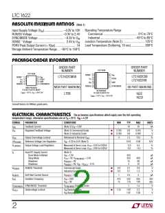
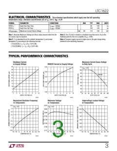
LTC1622
U
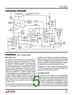
(Refer to Functional Diagram)
OPERATIO
the ITH pin will drop. When the ITH voltage goes below
0.12V, the sleep signal goes high, turning off the external
MOSFET. The sleep signal goes low when the ITH voltage
rises above 0.22V and the LTC1622 resumes normal
operation. The next oscillator cycle will turn the external
MOSFET on and the switching cycle repeats.
Short-Circuit Protection
Whentheoutputisshortedtoground, thefrequencyofthe
oscillator will be reduced to about 110kHz. This lower
frequency allows the inductor current to safely discharge,
thereby preventing current runaway. The oscillator’s fre-
quency will gradually increase to its nominal value when
the feedback voltage increases above 0.65V. Note that
synchronization is inhibited until the feedback voltage
goes above 0.3V.
Frequency Synchronization
The LTC1622 can be externally driven by a TTL/CMOS
compatibleclocksignalupto750kHz. Donot synchronize
the LTC1622 below its maximum default operating fre-
quency of 625kHz as this may cause abnormal operation
and an undesired frequency spectrum. The LTC1622 is
synchronized to the rising edge of the clock. The external
clock pulse width must be at least 100ns and not more
than the period minus 200ns.
Overvoltage Protection
As a further protection, the overvoltage comparator in the
LTC1622 will turn the external MOSFET off when the
feedback voltage has risen 7.5% above the reference
voltage of 0.8V. This comparator has a typical hysteresis
of 35mV.
Synchronization is inhibited when the feedback voltage is
below 0.3V. This is to prevent inductor current buildup
under short-circuit conditions. Burst Mode operation is
deactivated when the LTC1622 is externally driven by a
clock.
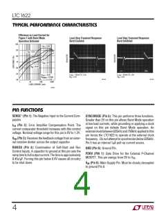
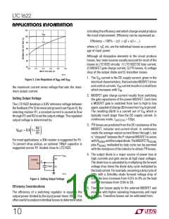
Slope Compensation and Peak Inductor Current
The inductor’s peak current is determined by:
V
ITH
I =
PK
10 R
Dropout Operation
SENSE
(
)
When the input supply voltage decreases towards the
output voltage, the rate of change of inductor current
during the ON cycle decreases. This reduction means that
the P-channel MOSFET will remain on for more than one
oscillator cycle since the inductor current has not ramped
up to the threshold set by EA. Further reduction in input
supplyvoltagewilleventuallycausetheP-channelMOSFET
tobeturnedon100%, i.e., DC. Theoutputvoltagewillthen
be determined by the input voltage minus the voltage drop
across the MOSFET, the sense resistor and the inductor.
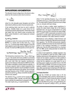
when the LTC1622 is operating below 40% duty cycle.
However, once the duty cycle exceeds 40%, slope com-
pensation begins and effectively reduces the peak induc-
torcurrent. Theamountofreductionisgivenbythecurves
in Figure 2.
110
100
90
80
70
60
Undervoltage Lockout
I
= 0.4I
PK
RIPPLE
50
40
30
20
10
AT 5% DUTY CYCLE
= 0.2I
TopreventoperationoftheP-channelMOSFETbelowsafe
input voltage levels, an undervoltage lockout is incorpo-
rated into the LTC1622. When the input supply voltage
drops below 2V, the P-channel MOSFET and all circuitry is
turned off except the undervoltage block, which draws
only several microamperes.
I
RIPPLE
PK
AT 5% DUTY CYCLE
V
IN
= 4.2V
UNSYNC
0
10 20 30 40 50 60 70 80 90 100
DUTY CYCLE (%)
1622 F02
Figure 2. Maximum Output Current vs Duty Cycle
6

 Linear [ Linear ]