LTC1622
U
W U U
APPLICATIONS INFORMATION
101
is limiting the efficiency and which change would produce
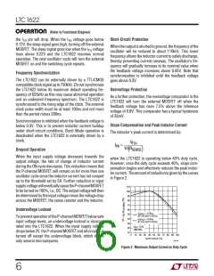
the most improvement. Efficiency can be expressed as:
V
REF
100
99
98
97
96
95
Efficiency = 100% – (η1 + η2 + η3 + ...)
V
ITH
where η1, η2, etc. are the individual losses as a percent-
age of input power.
Although all dissipative elements in the circuit produce
losses, four main sources usually account for most of the
losses in LTC1622 circuits: 1) LTC1622 DC bias current,
2) MOSFET gate charge current, 3) I2R losses, 4) voltage
drop of the output diode and 5) transition losses.
2.0
2.2
2.4
2.6
2.8
3.0
INPUT VOLTAGE (V)
1622 F03
1. The VIN current is the DC supply current, given in the
electricalcharacteristics, thatexcludesMOSFETdriver
and control currents. VIN current results in a small loss
which increases with VIN.
Figure 3. Line Regulation of VREF and VITH
the maximum current sense voltage that sets the maxi-
mum output current.
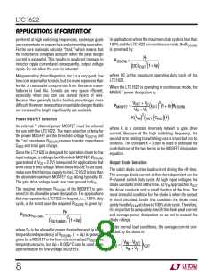
2. MOSFET gate charge current results from switching
the gate capacitance of the power MOSFET. Each time
a MOSFET gate is switched from low to high to low
again,apacketofchargedQmovesfromVIN toground.
The resulting dQ/dt is a current out of VIN which is
typically much larger than the DC supply current. In
continuous mode, IGATECHG = f(Qp).
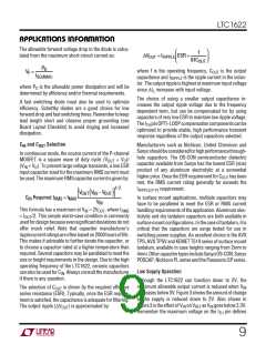
Setting Output Voltage
The LTC1622 develops a 0.8V reference voltage between
thefeedback(Pin3)terminalandground(seeFigure4).By
selecting resistor R1, a constant current is caused to flow
throughR1andR2tosettheoutputvoltage. Theregulated
output voltage is determined by:
3. I2R losses are predicted from the DC resistances of the
MOSFET, inductor and current shunt. In continuous
mode the average output current flows through L but
is “chopped” between the P-channel MOSFET in series
withRSENSE andtheoutputdiode.TheMOSFETRDS(ON)
plus RSENSE multiplied by duty cycle can be summed
with the resistance of the inductor to obtain I2R losses.
R2
R1
V
= 0.8 1+
OUT
For most applications, a 30k resistor is suggested for R1.
To prevent stray pickup, an optional 100pF capacitor is
suggested across R1 located close to LTC1622.
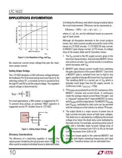
4. The output diode is a major source of power loss at
high currents and gets worse at high input voltages.
The diode loss is calculated by multiplying the forward
voltage drop times the diode duty cycle multiplied by
theloadcurrent. Forexample, assumingadutycycleof
50% with a Schottky diode forward voltage drop of
0.4V, the loss increases from 0.5% to 8% as the load
current increases from 0.5A to 2A.
V
OUT
R2
R1
LTC1622
3
V
FB
100pF
1622 F04
Figure 4. Setting Output Voltage
Efficiency Considerations
5. Transition losses apply to the external MOSFET and
increase with higher operating frequencies and input
voltages. Transition losses can be estimated from:
The efficiency of a switching regulator is equal to the
output power divided by the input power times 100%. It is
oftenusefultoanalyzeindividuallossestodeterminewhat
10

 Linear [ Linear ]