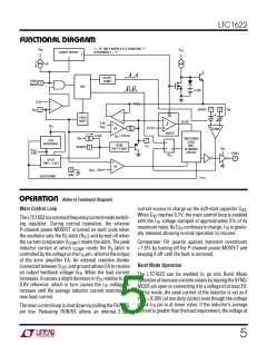
LTC1622
W
U
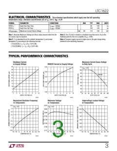
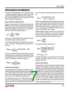
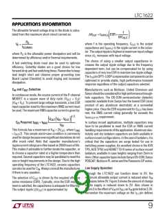
TYPICAL PERFORMANCE CHARACTERISTICS
Efficiency vs Load Current for
Figure 1 with Burst Mode
Operation Defeated
Load Step Transient Response
Burst Enabled
Load Step Transient Response
Burst Inhibited
100
90
80
70
60
50
40
V
= 3.3V
IN
V
= 4.2V
IN
V
= 6V
IN
V
= 8.4V
IN
ILOAD = 50mA TO 1.2A
VIN = 4.2V
ILOAD = 50mA TO 1.2A
VIN = 4.2V
V
R
= 2.5V
= 0.03Ω
OUT
SENSE
1622 G08
1622 G09
1
10
100
1000
LOAD CURRENT (mA)
1622 G07
U
U
U
PIN FUNCTIONS
SENSE– (Pin 1): The Negative Input to the Current Com-
parator.
SYNC/MODE (Pin 5): This pin performs three functions.
Greater than 2V on this pin allows Burst Mode operation
at low load currents, while grounding or applying a clock
signal on this pin defeats Burst Mode operation. An
external clock between 625kHz and 750kHz applied to this
pin forces the LTC1622 to operate at the external clock
frequency. Do not attempt to synchronize below 625kHz.
Pin 5 has an internal 1µA pull-up current source.
ITH (Pin 2): Error Amplifier Compensation Point. The
current comparator threshold increases with this control
voltage. Nominal voltage range for this pin is 0V to 1.2V.
VFB (Pin 3): Receives the feedback voltage from an exter-
nal resistive divider across the output capacitor.
RUN/SS (Pin 4): Combination of Soft-Start and Run
Control Inputs. A capacitor to ground at this pin sets the
ramptimetofulloutputcurrent. Thetimeisapproximately
0.45s/µF. Forcing this pin below 0.4V causes all circuitry
to be shut down.
GND (Pin 6): Ground Pin.
PDRV (PIN 7): Gate Drive for the External P-Channel
MOSFET. This pin swings from 0V to VIN.
VIN (Pin 8): Main Supply Pin. Must be closely decoupled
to ground Pin 6.
4

 Linear [ Linear ]