LTC1622
U
W U U
APPLICATIONS INFORMATION
Transition Loss = 3(VIN)2IO(MAX) RSS
(f)
C
V
OUT
LTC1622
R2
R1
Other losses including CIN and COUT ESR dissipative
losses, and inductor core losses, generally account for
less than 2% total additional loss.
+
I
V
FB
TH
D
FB
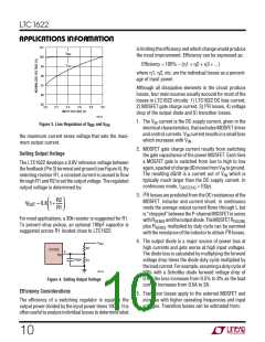
Run/Soft-Start Function
1622 F05
The RUN/SS pin is a dual purpose pin that provides the
soft-startfunctionandameanstoshutdowntheLTC1622.
Soft-start reduces input surge current from VIN by gradu-
ally increasing the internal current limit. Power supply
sequencing can also be accomplished using this pin.
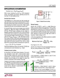
Figure 5. Foldback Current Limiting
Design Example
Assume the LTC1622 is used in a single lithium-ion
battery-poweredcellularphoneapplication.TheVIN willbe
operating from a maximum of 4.2V down to a minimum of
2.7V. Load current requirement is a maximum of 1.5A but
most of the time it will be on standby mode, requiring only
2mA. Efficiency at both low and high load current is
important. Output voltage is 2.5V.
An internal 2.5µA current source charges up an external
capacitor CSS. When the voltage on the RUN/SS reaches
0.7V the LTC1622 begins operating. As the voltage on
RUN/SS continues to ramp from 0.7V to 1.8V, the internal
current limit is also ramped at a proportional linear rate.
The current limit begins near 0A (at VRUN/SS = 0.7V) and
ends at 0.1/RSENSE (VRUN/SS ≥ 1.8V). The output current
thus ramps up slowly, reducing the starting surge current
required from the input power supply. If the RUN/SS has
been pulled all the way to ground, there will be a delay
before the current limit starts increasing and is given by:
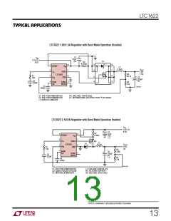
In the above application, Burst Mode operation is enabled
by connecting Pin 5 to VIN.
V
+ V
D
+ V
D
OUT
Maximum Duty Cycle =
= 93%
V
IN(MIN)
t
DELAY = 2.8 • 105 • CSS in seconds
From Figure 2, SF = 57%.
Pulling the RUN/SS pin below 0.4V puts the LTC1622 into
a low quiescent current shutdown (IQ < 15µA).
Use the curve of Figure 2 since the operating frequency is
the free running frequency of the LTC1622.
Foldback Current Limiting
SF
0.57
RSENSE
=
=
= 0.0253Ω
As described in the Output Diode Selection, the worst-
case dissipation occurs with a short-circuited output
when the diode conducts the current limit value almost
continuously. To prevent excessive heating in the diode,
foldback current limiting can be added to reduce the
current in proportion to the severity of the fault.
15
100
15 1.5A
( )(
I
( )( OUT)(
)
)
In the application, a 0.025Ω resistor is used. For the
inductor, the required value is:
4.2 − 2.5
0.036
2.5 + 0.3
4.2 + 0.3
L
=
= 1.33µH
MIN
Foldback current limiting is implemented by adding diode
DFB (1N4148orequivalent)betweentheoutputandtheITH
pin as shown in Figure 5. In a hard short (VOUT = 0V), the
current will be reduced to approximately 50% of the
maximum output current.
550kHz
0.025
In the application, a 3.9µH inductor is used to reduce
inductor ripple current and thus, output voltage ripple.
For the selection of the external MOSFET, the RDS(ON)
mustbeguaranteedat2.5VsincetheLTC1622hastowork
11

 Linear [ Linear ]