LTC1622
U
U W
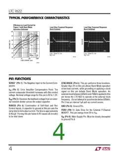
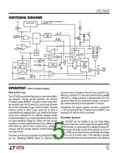
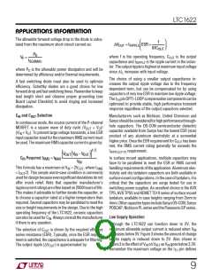
FUNCTIONAL DIAGRA
Y = “0” ONLY WHEN X IS A CONSTANT “1”
OTHERWISE Y = “1”
V
IN
V
CC
BURST DEFEAT
Y
X
1µA
SLOPE
COMP
SYNC/
5
MODE
OSC
0.36V
0.3V
–
–
V
IN
1
+
8
SENSE
V
3
FB
–
+
EN
FREQ
–
+
SHIFT
SLEEP
0.8V
REF
+
V
IN
V
+
–
0.12V
EA
ICOMP
–
BURST
Ω
g
m
= 0.5m
2.5µA
V
IN
SWITCHING
0.8V
REFERENCE
2
LOGIC
AND
S
RUN/
I
TH
RUN/SS
4
V
SOFT-START
R
Q
BLANKING
CIRCUIT
IN
V
REF
0.8V
PDRV
7
R
S1
UVLO
TRIP = 1.97V
+
OV
6
V
+ 60mV
–
REF
GND
SHUTDOWN
1622 BD
U
(Refer to Functional Diagram)
OPERATIO
Main Control Loop
current source to charge up the soft-start capacitor CSS.
When CSS reaches 0.7V, the main control loop is enabled
with the ITH voltage clamped at approximately 5% of its
maximum value. As CSS continues to charge, ITH is gradu-
ally released allowing normal operation to resume.
TheLTC1622isaconstantfrequencycurrentmodeswitch-
ing regulator. During normal operation, the external
P-channel power MOSFET is turned on each cycle when
the oscillator sets the RS latch (RS1) and turned off when
the current comparator (ICOMP) resets the latch. The peak
inductor current at which ICOMP resets the RS latch is
controlledbythevoltageontheITH pin, whichistheoutput
of the error amplifier EA. An external resistive divider
connected between VOUT and ground allows EA to receive
an output feedback voltage VFB. When the load current
increases, it causes a slight decrease in VFB relative to the
0.8V reference, which in turn causes the ITH voltage to
increase until the average inductor current matches the
new load current.
Comparator OV guards against transient overshoots
>7.5% by turning off the P-channel power MOSFET and
keeping it off until the fault is removed.
Burst Mode Operation
The LTC1622 can be enabled to go into Burst Mode
operationatlowloadcurrentssimplybyleavingtheSYNC/
MODE pin open or connecting it to a voltage of at least 2V.
In this mode, the peak current of the inductor is set as if
VITH = 0.36V (at low duty cycles) even though the voltage
at the ITH pin is at lower value. If the inductor’s average
current is greater than the load requirement, the voltage at
The main control loop is shut down by pulling the RUN/SS
pin low. Releasing RUN/SS allows an internal 2.5µA
5

 Linear [ Linear ]