LT3587
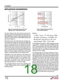
APPLICATIONS INFORMATION
Output Disconnect
The output disconnect feature on Boost3 is implemented
similarlyusingM3. However, inthiscaseM3isonlyturned
off when the EN/SS3 pin voltage is less than 200mV and
the Boost3 regulation loop is disabled.
Both the Boost1 and the Boost3 channels have an output
disconnect between their respective CAP pin and V
OUT
IN
pin. This disconnect feature prevents a DC path from V
to V
.
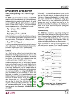
The disconnect transistor M3 is also current limited, pro-
OUT
vidingamaximumoutputcurrentatV
of110mA(typ).
OUT3
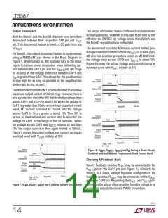
ForBoost1, thisoutputdisconnectfeatureisimplemented
using a PMOS (M1) as shown in the Block Diagram in
Figure 1. When turned on, M1 is driven hard in the linear
region to reduce power dissipation when delivering cur-
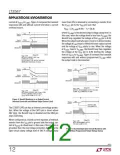
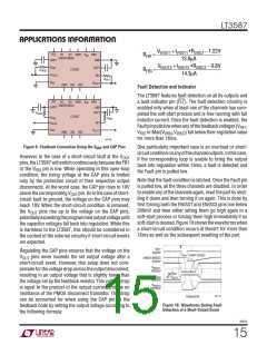
M3 also has a similar protection circuit as M1 that limits
the voltage drop across CAP3 and V to about 10V.
OUT3
Figure 8 shows the output voltage and current during an
overload event with V initially at 24V.
CAP3
rent between the CAP1 pin and the V
pin. M1 stays
OUT1
on as long as the voltage difference between CAP1 and
V is greater than 2.5V. This allows for the positive bias
IN
I
VOUT3
to stay high for as long as possible as the negative bias
500mA/DIV
0mA
24V
discharges during turn off.
I
L4
500mA/DIV
ThedisconnecttransistorM1iscurrentlimitedtoprovidea
maximumoutputcurrentof155mA(typ).However,thereis
also a protection circuit for M1 that limits the voltage drop
V
CAP3
10V/DIV
V
VOUT3
10V/DIV
across CAP1 and V
to about 10V. When the voltage at
OUT1
CAP1 is greater than 10V, in an overload or a short-circuit
3587 F08a
40μs/DIV
event, M1 current is limited to 155mA until the voltage
across CAP1 to V
grows to about 10V. Then M1 is
OUT1
I
VOUT3
turned on hard without any current limit to allow for the
voltage on CAP1 to discharge as fast as possible. When
500mA/DIV
0mA
I
L4
the voltage across CAP1 and V
reduces to less than
500mA/DIV
OUT1
10V, the output current is then again limited to 155mA.
Figure 7 shows the output voltage and current during an
V
CAP3
24V
10V/DIV
V
VOUT3
overload event with V
initially at 15V.
CAP1
10V/DIV
3587 F08b
40μs/DIV
V
= 3.6V
VIN
C4 = 1μF
I
VOUT1
Figure 8. VCAP3, VVOUT3, IVOUT3 and IL4 During a Short-Circuit
Condition with and Without Programmed 20mA Current Limit
500mA/DIV
0mA
I
L1
500mA/DIV
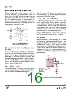
Choosing A Feedback Node
V
CAP1
15V
15V
10V/DIV
Boost1 feedback resistor, R , may be connected to the
FB1
V
VOUT1
V
pin or the CAP1 pin (see Figure 9). Similarly for
OUT1
10V/DIV
Boost3 in a boost voltage regulator configuration, the
3587 F07
40μs/DIV
V
VIN
= 3.6V
C1 = 4.7μF
feedback resistor, R
, may be connected to the V
VFB3
OUT3
pins
pin or the CAP3 pin. Regulating the V
and V
OUT1
OUT3
Figure 7. VCAP1,VVOUT1, IVOUT1 and IL1 During a Short-Circuit Event
eliminatestheoutputoffsetresultingfromthevoltagedrop
across the output disconnect PMOS transistors.
3587fc
14

 Linear [ Linear ]