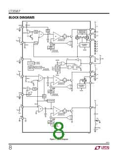
LT3587
APPLICATIONS INFORMATION
capacitancewillslowdowntheswitchingwaveform,which
can cause significant switching losses at 1MHz switch-
ing frequency. Some recommended Schottky diodes are
listed in Table 2.
The same constraints as the other Schottky diodes ap-
ply for selecting D3. Therefore, the same recommended
Schottky diodes in Table 2 can be used for D3.
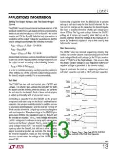
Boost3 Overcurrent and Overvoltage Protection
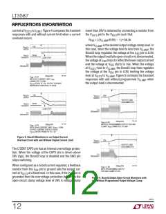
Table 2. Recommended Schottky Diodes
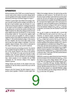
As briefly discussed in the Operation section, the regula-
tion loop of Boost3 uses the maximum of the two voltages
at V and I as feedback information to set the peak
current of its power switch Q3. This allows for the Boost3
loop to be configured as either a boost voltage regulator
or a boost current regulator (Figure 3). Furthermore, this
architecturealsoallowsforaprogrammablecurrentlimiton
voltage regulation or voltage limit on current regulation.
DIODE
FORWARD FORWARD CAPACI-
PART
NUMBER
CURRENT VOLTAGE
TANCE
FB3
FB3
(mA)
DROP (V) (pF at 10V) MANUFACTURER
RSX051VA-30
1000
0.35
30
ROHM
www.rohm.com
PMEG401OCEJ
PMEG2005EB
IR05H40CSPTR
500
500
500
0.49
0.43
0.48
25
8
NXP/Phillips
www.nxp.com
39
Vishay
www.vishay.com
V
V
VIN
VIN
B0540WS
ZLLS400
500
520
0.48
0.53
20
17
Diodes Inc.
www.diodes.com
V
SW3
CAP3
V
SW3
CAP3
IN
IN
Zetex
www.zetex.com
LT3587
BOOST3
VOLTAGE
LT3587
BOOST3
V
V
OUT3
OUT3
CURRENT
REGULATOR
R
R
VFB3
VFB3
REGULATOR
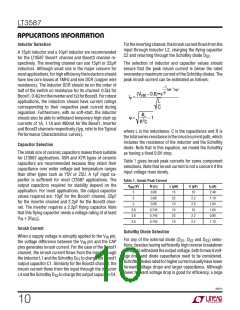
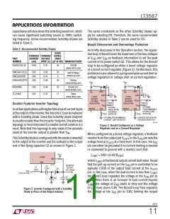
Smaller Footprint Inverter Topology
V
V
FB3
FB3
OPTIONAL
VOLTAGE
I
I
FB3
FB3
EN/SS3
EN/SS3
PROGRAMMABLE
VOLTAGE LIMIT
RESISTOR
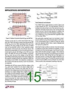
Incertainapplicationswithhighertoleranceofcurrentripple
attheoutputoftheinverter,theinductorL3canbereplaced
with a Schottky diode. Since the Schottky diode footprint
isusuallysmallerthantheinductorfootprint,thisalternate
topology is recommended if a smaller overall solution is a
must. Note that this topology is only viable if the absolute
REGULATION
FEEDBACK
RESISTOR
R
IFB3
R
IFB3
CURRENT REGULATION
FEEDBACK RESISTOR
3587 F03
OPTIONALPROGRAMMABLE
CURRENT LIMIT RESISTOR
Figure 3. Boost3 Configured as a Voltage
Regulator and as a Current Regulator
value of the inverter output is greater than V .
IN
When configured as a boost voltage regulator, a feedback
resistor from the output pin V to the V pin sets the
ThisSchottkydiodeisconfiguredwiththeanodeconnected
to the output of the inverter and the cathode to the output
end of the flying capacitor C2 as shown in Figure 2.
OUT3
FB3
voltage level at V
at a fixed level. In this case, the I
OUT3
FB3
pin can either be grounded if no current limiting is desired
or connected to ground with a resistor such that:
R
FB1
I
= 200 • (0.8V/R
)
LIMIT
IFB3
1M
LT3587
SW2
FB2
whereI
isthedesiredoutputcurrentlimitvalue.Recall
LIMIT
3587 F02
that the pull-up current on the I pin is controlled to be
FB3
INVERTER
OUTPUT
C2
2.2μF
L2
15μH
typically 1/200 of the output load current at the V
D3
OUT3
–8V, 100mA
V
VIN
pin. In this case, when the load current is less than I
,
2.5V TO 4.5V
LIMIT
the Boost3 loop regulates the voltage at the V
pin to
C7
22μF
FB3
DS2
0.8V. When there is an increase in load current beyond
, the voltage at V starts to drop and the voltage
I
LIMIT
FB3
at I rises above 0.8V. The Boost3 loop then regulates
FB3
Figure 2. Inverter Configured with a Schottky
Diode in Place of the Output Inductor
the voltage at the I
pin to 0.8V, limiting the output
FB3
3587fc
11

 Linear [ Linear ]