LT3587
APPLICATIONS INFORMATION
Setting The Output Voltages and The Boost3 Output
Current
Connecting a capacitor from the EN/SS3 pin to ground
sets up a soft-start ramp for the Boost3 channel. As the
1μA current charges up the capacitor, the Boost3 regula-
tion loop is enabled when the EN/SS3 pin voltage goes
The LT3587 has a trimmed internal feedback resistor. A 1M
feedbackresistorfromeachoutputpintoitscorresponding
feedbackpinsetstheoutputsto15VforBoost1,–8Vforthe
inverter and 15V for Boost3. Note that only one resistor is
needed to set the output voltage for each channel. Set the
output voltages according to the following formulas:
above 200mV. The V node voltage follows the EN/SS3
C3
voltage as it ramps up ensuring slow start-up on the
Boost3 channel. When the voltage at the EN/SS3 pin is
above 2V, the Boost3 regulation loop is free running with
full inductor current.
R
R
= ((V
/1.22V) – 1) • 88.5k
FB1
FB2
VOUT1
Start Sequencing
= |V |/8μA
NEG
The LT3587 also has internal sequencing circuitry that
inhibits the inverter channel from operating until the feed-
backvoltageoftheBoost1voltage(attheFB1pin)reaches
about 1.1V (87% of the final voltage). This ensures that
the Boost1 output voltage is near regulation before any
negative voltage is generated at the inverter output.
R
= ((V
/0.8V) – 1) • 56.3k
VFB3
VOUT3
Asdescribedinprevioussections,Boost3canbeconfigured
as a boost current regulator. When configured as such, set
the output current according to the following formula:
R
= 200 • (0.8V/I
)
IFB3
VOUT3
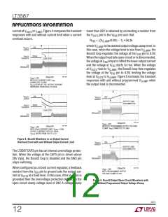
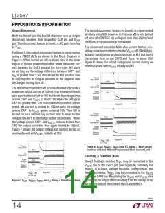
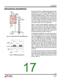
Figure 6 contrasts the start-up sequencing without any
soft-start capacitor, and with a 10nF soft-start capacitor.
Inordertomaintainaccuracy, usehighprecisionresistors
when setting any of the channels output voltage and/or
the Boost3 output current (1% is recommended).
Soft-Start
V
EN/SS1
0V
2V/DIV
The LT3587 has two soft-start control pins: EN/SS1 and
EN/SS3. The EN/SS1 pin controls the soft-start for both
the Boost1 and the inverter, while the EN/SS3 pin controls
the soft-start for the Boost3. Each of these soft-start pins
is pulled up internally with a 1μA current source.
I
VIN
0mA
500mA/DIV
V
VOUT1
10V/DIV
0V
0V
V
NEG
10V/DIV
Connecting a capacitor from the EN/SS1 pin to ground
programs a soft-start ramp for the Boost1 and the inverter
channels. Use an open-drain transistor to pull this pin low
to shut down both the Boost1 and the inverter. Turning off
this transistor allows the 1μA pull-up current to charge the
soft-start capacitor. When the voltage at the EN/SS1 pins
goes above 200mV, the regulation loops for Boost1 and
3587 F06a
400μs/DIV
V
EN/SS1
2V/DIV
I
VIN
0mA
500mA/DIV
the inverter are enabled. The V node voltage follows the
C1
V
VOUT1
0V
0V
10V/DIV
EN/SS1 voltage as it continues to ramp up to ensure slow
V
NEG
start-up on the Boost1 channel. The V node follows the
C2
10V/DIV
ramp voltage minus 0.7V. This ensures that the inverter
starts up after the Boost1, but still has a slow ramping
output to avoid large start-up currents. The Boost1 and
the inverter regulation loops are free running with full
inductor current when the voltage at the EN/SS1 pin is
above 2.5V.
3587 F06b
4ms/DIV
Figure 6. VEN/SS1, VOUT1, VNEG, IVIN with No Soft-Start
Capacitor, and with a 10nF Soft-Start Capacitor
3587fc
13

 Linear [ Linear ]