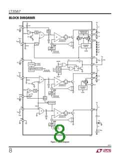
LT3587
APPLICATIONS INFORMATION
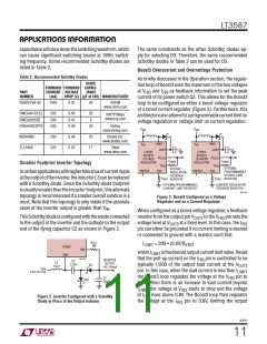
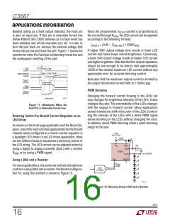
current at V
to I . Figure 4 compares the transient
LIMIT
lower than 29V is obtained by connecting a resistor from
the V pin to the V pin such that:
OUT3
responses with and without current limit when a current
overload occurs.
OUT3
FB3
R
FB3
= ((V
/0.8V) – 1) • 56.3k
CLAMP
where V
is the desired output voltage clamp level. In
CLAMP
15V
V
VOUT3
5V/DIV
this case, when the voltage level is less than V
, the
CLAMP
Boost3 loop regulates the voltage at the I pin to 0.8V.
FB3
I
20mA
VOUT3
Whentheoutputloadfailsopen-circuitorisdisconnected,
13mA/DIV
LOAD STEP
the voltage at I drops to reflect the lower output current
FB3
I
L4
and the voltage at V
starts to rise. When the voltage
, the Boost3 loop then regulates
FB3
CLAMP
200mA/DIV
at V
rises to V
OUT3
the voltage at the V
pin to 0.8V, limiting the voltage
. Figure 5 contrasts the transient
FB3
CLAMP
3587 F04a
level at V
to V
200μs/DIV
OUT3
V
= 3.6V
VIN
WITHOUT CURRENT LIMIT: I
CONNECTED TO GND
FB3
responses with and without programmed V
the output load is disconnected.
when
CLAMP
V
STAYS AT 15V, OUTPUT CURRENT
OUT3
INCREASES FROM 20mA TO 40mA
15V
V
VOUT3
20V
V
VOUT3
5V/DIV
10V/DIV
OUTPUT LOAD
DISCONNECTED
I
20mA
VOUT3
13mA/DIV
LOAD STEP
I
L4
200mA/DIV
I
L4
200mA/DIV
3587 F05a
200μs/DIV
WITHOUT PROGRAMMED OUTPUT VOLTAGE
CLAMP: V CONNECTED TO GND
V
= 3.6V
VIN
3587 F04b
200μs/DIV
V
= 3.6V
VIN
FB3
WITH 20mA CURRENT LIMIT: R
OUTPUT CURRENT STAYS AT 20mA,
DROPS FROM 15V TO 7.5V
= 8.06k
IFB3
V
OUT3
Figure 4. Boost3 Waveform in an Output Current
Overload Event with and Without Output Current Limit
20V
V
VOUT3
10V/DIV
OUTPUT LOAD
DISCONNECTED
The LT3587 CAP3 pin has an internal overvoltage protec-
tion. When the voltage at the CAP3 pin is driven above
29V (typ), the Boost3 loop is disabled and the SW3 pin
stops switching.
I
L4
200mA/DIV
3587 F05b
When configured as a boost current regulator, a feedback
200μs/DIV
V
= 3.6V
VIN
WITH PROGRAMMED OUTPUT
VOLTAGE CLAMP AT 24V
resistor from the I pin to ground sets the output cur-
FB3
rent at V
at a fixed level. In this case, if the V pin is
grounded then the overvoltage protection defaults to the
OUT3
FB3
Figure 5. Boost3 Output Open-Circuit Waveform with
and Without Programmed Output Voltage Clamp
open-circuit clamp voltage level of 29V. A voltage clamp
3587fc
12

 Linear [ Linear ]