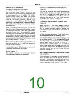
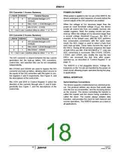
X96010
VOLTAGE REFERENCE
A/D CONVERTER
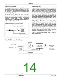
The voltage reference to the A/D and D/A converters
on the X96010, may be driven from the on-chip volt-
age reference, or from an external source via the VRef
pin. Bit VRM in Control Register 0 selects between the
two options (See Figure 5).
The X96010 contains a general purpose, on-chip, 8-bit
Analog to Digital (A/D) converter whose output is avail-
able at the Status Register as bits AD[7:0]. By default
these output bits are used to select a row in the look-
up tables associated with the X96010’s Current Gen-
erators. When bit ADCfiltOff is “0” (default), bits
AD[7:0] are updated each time the ADC performs four
consecutive conversions with the same exact result at
the 6 MSBs. When bit ADCfiltOff is “1”, these bits are
updated after every ADC conversion.
The default value of VRM is “0”, which selects the
internal reference. When the internal reference is
selected, it’s output voltage is also an output at pin
VRef with a nominal value of 1.21 V. If an external
voltage reference is preferred, the VRM bit of the Con-
trol Register 0 must be set to “1”.
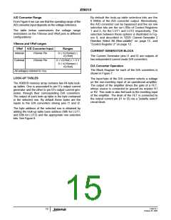
A block diagram of the A/D converter is shown in Fig-
ure 6. The voltage reference input (see “VOLTAGE
REFERENCE” for details), sets the maximum ampli-
tude of the ramp generator output. The A/D converter
input signal (see “A/D Converter Input Select” below
for details) is compared to the ramp generator output.
The control and encode logic produces a binary
encoded output, with a minimum value of 00h (010),
and a full scale output value of FFh (25510).
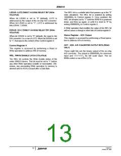
Figure 5. Voltage Reference Structure
VRM: bit 2 in Control register 0.
On-chip
Voltage
VRef Pin
Reference
The A/D converter input voltage range (VIN
from 0 V to V(VRef).
) is
ADC
A/D Converter and
D/A Converters reference
Figure 6. A/D Converter Block Diagram
Comparator
VSense Pin
From VRef
8
Control and
Encode Logic
A/D Converter
Output
(To LUTs and
Status Register)
Ramp
Generator
Conversion Reset
Clock
FN8214.1
14
October 25, 2005

 INTERSIL [ Intersil ]