X96010
L2DAS: LUT2 DIRECT ACCESS SELECT BIT (NON-
VOLATILE)
The WEL bit is a volatile latch that powers up in the “0”
state (disabled). The WEL bit is enabled by writing
10000000 to Control register 6. Once enabled, the
WEL bit remains set to “1” until the X96010 is powered
down, and then up again, or until it is reset to “0” by
2
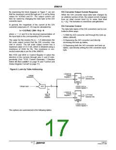
When bit L2DAS is set to “0” (default), LUT2 is
addressed by the output of the on-chip A/D converter.
When bit L2DAS is set to “1”, LUT2 is addressed by
bits L2DA5 - L2DA0.
writing 00000000 to Control register 6.
2
A Write operation that modifies the value of the WEL bit
will not cause a change in other bits of Control register 6.
D2DAS: D/A 2 DIRECT ACCESS SELECT BIT (NON-
VOLATILE)
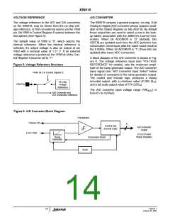
Status Register - ADC Output
When bit D2DAS is set to “0” (default), the input to the
D/A converter 2 is a row of LUT2. When bit D2DAS is set
to “1”, that input is the content of the Control register 4.
This register is accessed by performing a Read opera-
tion to address 87h of memory.
AD7 - AD0: A/D CONVERTER OUTPUT BITS (READ
ONLY)
Control Register 6
This register is accessed by performing a Read or
Write operation to address 86h of memory.
These eight bits are the binary output of the on-chip
A/D converter. The output is 00000000 for minimum
2
WEL: WRITE ENABLE LATCH (VOLATILE)
input and 11111111 for full scale input. The six
2
MSBs select a row of the LUTs.
The WEL bit controls the Write Enable status of the
entire X96010 device. This bit must be set to “1” before
any other Write operation (volatile or nonvolatile). Oth-
erwise, any proceeding Write operation to memory is
aborted and no ACK is issued after a Data Byte.
FN8214.1
13
October 25, 2005

 INTERSIL [ Intersil ]