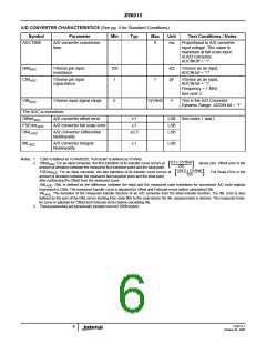
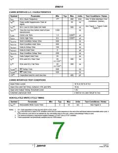
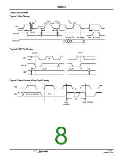
X96010
PRINCIPLES OF OPERATION
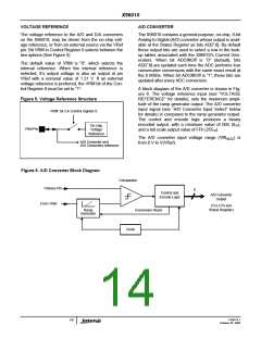
VRM: VOLTAGE REFERENCE PIN MODE (NON-
VOLATILE)
CONTROL AND STATUS REGISTERS
The VRM bit configures the Voltage Reference pin
(VRef) as either an input or an output. When the VRM
bit is set to “0” (default), the voltage at pin VRef is an
output from the X96010’s internal voltage reference.
When the VRM bit is set to “1”, the voltage reference
for the VRef pin is external. See Figure 5.
The Control and Status Registers provide the user
with a mechanism for changing and reading the value
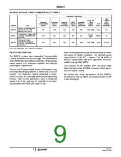
of various parameters of the X96010. The X96010
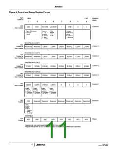
contains seven Control, one Status, and several
Reserved registers, each being one Byte wide (See
Figure 4). The Control registers 0 through 6 are
located at memory addresses 80h through 86h
respectively. The Status register is at memory address
87h, and the Reserved registers at memory address
88h through 8Fh.
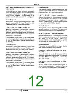
ADCFILTOFF: ADC FILTERING CONTROL (NON-
VOLATILE)
When this bit is“1”, the status register at 87h is
updated after every conversion of the ADC. When this
bit is “0” (default), the status register is updated after
four consecutive conversions with the same result, on
the 6 MSBs.
All bits in Control register 6 always power-up to the logic
state “0”. All bits in Control registers 0 through 5 power-
up to the logic state value kept in their corresponding
nonvolatile memory cells. The nonvolatile bits of a reg-
ister retain their stored values even when the X96010 is
powered down, then powered back up. The nonvolatile
bits in Control 0 through Control 5 registers are all pre-
programmed to the logic state “0” at the factory, except
the cases that indicate “1” in Figure 4.
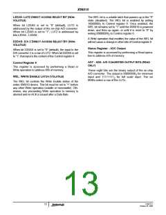
NV1234: CONTROL REGISTERS 1, 2, 3, AND 4 VOLA-
TILITY MODE SELECTION BIT (NON-VOLATILE)
When the NV1234 bit is set to “0” (default), bytes writ-
ten to Control registers 1, 2, 3, and 4 are stored in vol-
atile cells, and their content is lost when the X96010 is
powered down. When the NV1234 bit is set to “1”,
bytes written to Control registers 1, 2, 3, and 4 are
stored in both volatile and nonvolatile cells, and their
value doesn’t change when the X96010 is powered
down and powered back up. See “Writing to Control
Registers” on page 23.
Bits indicated as “Reserved” are ignored when read,
and must be written as “0”, if any Write operation is
performed to their registers.
A detailed description of the function of each of the
Control and Status register bits follows:
Control Register 0
I1DS: CURRENT GENERATOR 1 DIRECTION SELECT BIT
(NON-VOLATILE)
This register is accessed by performing a Read or
Write operation to address 80h of memory.
The I1DS bit sets the polarity of Current Generator 1,
DAC1. When this bit is set to “0” (default), the Current
Generator 1 of the X96010 is configured as a Current
Source. Current Generator 1 is configured as a Cur-
rent Sink when the I1DS bit is set to “1”. See Figure 7.
FN8214.1
10
October 25, 2005

 INTERSIL [ Intersil ]