X96010
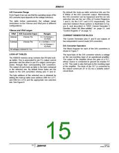
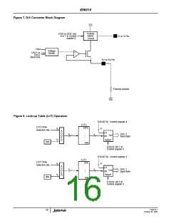
Figure 7. D/A Converter Block Diagram
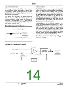
Vcc
Polarity
Select
Circuit
I1DS or I2DS: bits
6 or 7 in Control
register 0.
I1 or I2 Pin
VRef
Voltage
Divider
+
DAC1 or
DAC2
Input byte
-
R1 or R2 Pin
External resistor
Vss
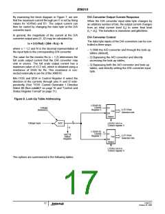
Figure 8. Look-up Table (LUT) Operation
D2DA[7:0] : Control register 4
8
LUT2
10Fh
LUT2 Row
6
Selection bits
A
D1
D
D
E
DAC 2
Out
8
8
D0
Input Byte
8
Select
R
D0h
D0h
D2DAS: Bit 7 of
Control register 5
D1DA[7:0] : Control register 3
8
LUT1
LUT1 Row
6
CFh
Selection bits
A
D1
D
D
E
DAC 1
Out
8
8
D0
Input Byte
8
Select
R
90h
90h
D1DAS: Bit 5 of
Control register 5
FN8214.1
16
October 25, 2005

 INTERSIL [ Intersil ]