X96010
I2DS: CURRENT GENERATOR 2 DIRECTION SELECT BIT
(NON-VOLATILE)
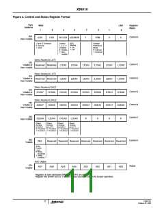
Control Register 3
This register is accessed by performing a Read or Write
operation to address 83h of memory. This byte’s volatility
is determined by bit NV1234 in Control register 0.
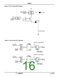
The I2DS bit sets the polarity of Current Generator 2,
DAC2. When this bit is set to “0” (default), the Current
Generator 2 of the X96010 is configured as a Current
Source. Current Generator 2 is configured as a Cur-
rent Sink when the I2DS bit is set to “1”. See Figure 7.
D1DA7 - D1DA0: D/A 1 DIRECT ACCESS BITS
When bit D1DAS (bit 5 in Control register 5) is set to
“1”, the input to the D/A converter 1 is the content of
bits D1DA7 - D1DA0, and it is not a row of LUT1.
When bit D1DAS is set to “0” (default) these eight bits
are ignored by the X96010. See Figure 8.
Control Register 1
This register is accessed by performing a Read or Write
operation to address 81h of memory. This byte’s volatility
is determined by bit NV1234 in Control register 0.
Control Register 4
L1DA5 - L1DA0: LUT1 DIRECT ACCESS BITS
This register is accessed by performing a Read or Write
operation to address 84h of memory. This byte’s volatil-
ity is determined by bit NV1234 in Control register 0.
When bit L1DAS (bit 4 in Control register 5) is set to
“1”, LUT1 is addressed by these six bits, and it is not
addressed by the output of the on-chip A/D converter.
When bit L1DAS is set to “0”, these six bits are ignored
by the X96010. See Figure 9.
D2DA7 - D2DA0: D/A 2 DIRECT ACCESS BITS
When bit D2DAS (bit 7 in Control register 5) is set to
“1”, the input to the D/A converter 1 is the content of
bits D2DA7 - D2DA0, and it is not a row of LUT2.
When bit D2DAS is set to “0” (default) these eight bits
are ignored by the X96010. (See Figure 8).
A value between 00h (0010) and 3Fh (6310) may be writ-
ten to these register bits, to select the corresponding row
in LUT1. The written value is added to the base address
of LUT1 (90h).
Control Register 5
Control Register 2
This register is accessed by performing a Read or
Write operation to address 85h of memory.
This register is accessed by performing a read or write
operation to address 82h of memory. This byte’s vola-
tility is determined by bit NV1234 in Control register 0.
L1DAS: LUT1 DIRECT ACCESS SELECT BIT (NON-
VOLATILE)
L2DA5 - L2DA0: LUT2 DIRECT ACCESS BITS
When bit L1DAS is set to “0” (default), LUT1 is
addressed by the output of the on-chip A/D converter.
When bit L1DAS is set to “1”, LUT1 is addressed by
bits L1DA5 - L1DA0.
When bit L2DAS (bit 6 in Control register 5) is set to
“1”, LUT2 is addressed by these six bits, and it is not
addressed by the output of the on-chip A/D converter.
When bit L2DAS is set to “0”, these six bits are ignored
by the X96010. See Figure 9.
D1DAS: D/A 1 DIRECT ACCESS SELECT BIT (NON-
VOLATILE)
A value between 00h (0010) and 3Fh (6310) may be writ-
ten to these register bits, to select the corresponding row
in LUT2. The written value is added to the base address
of LUT2 (D0h).
When bit D1DAS is set to “0” (default), the input to the
D/A converter 1 is a row of LUT1. When bit D1DAS is set
to “1”, that input is the content of the Control register 3.
FN8214.1
12
October 25, 2005

 INTERSIL [ Intersil ]