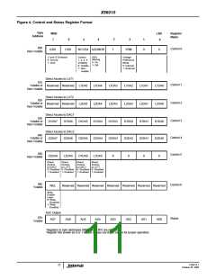
X96010
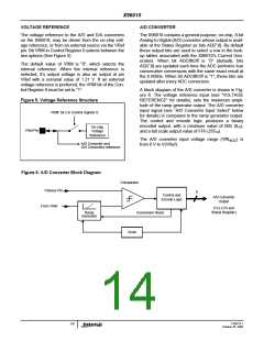
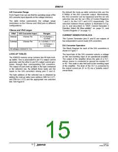
A/D Converter Range
By default the look-up table selection bits are the
6 MSBs of the A/D converter output. Alternatively,
the A/D converter can be bypassed and the six row
selection bits are the six LSBs of Control Registers
1 and 2, for the LUT1 and LUT2 respectively. The
selection between these options is illustrated in Fig-
ure 9, and described in “I2DS: Current Generator 2
Direction Select Bit (Non-volatile)” on page 12, and
“Control Register 2” on page 12.
From Figure 6 we can see that the operating range of the
A/D converter input depends on the voltage reference.
The table below summarizes the voltage range
restrictions on the VSense and VRef pins in different
configurations :
VSense and VRef ranges
VRef
A/D Converter Input
Ranges
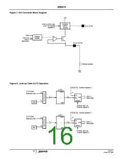
CURRENT GENERATOR BLOCK
Internal
VSense Pin
0 ≤ V(VSense) ≤
The Current Generator pins I1 and I2 are outputs of
two independent current mode D/A converters.
V(VRef)
External
VSense Pin
0 ≤ V(VRef) ≤ 1.3 V
0 ≤ V(VSense) ≤
D/A Converter Operation
V(VRef)
The Block Diagram for each of the D/A converters is
shown in Figure 7.
All voltages referred to Vss.
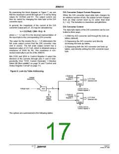
LOOK-UP TABLES
The input byte of the D/A converter selects a voltage
on the non-inverting input of an operational amplifier.
The output of the amplifier drives the gate of a FET,
whose source is connected to ground via resistor R1
or R2. This node is also fed back to the inverting input
of the amplifier. The drain of the FET is connected to
the output current pin (I1 or I2) via a “polarity select”
circuit block.
The X96010 memory array contains two 64-byte look-
up tables. One is associated to pin I1’s output current
generator and the other to pin I2’s output current gen-
erator, through their corresponding D/A converters.
The output of each look-up table is the byte contained
in the selected row. By default these bytes are the
inputs to the D/A converters driving pins I1 and I2.
The byte address of the selected row is obtained by
adding the look-up table base address (90h for LUT1,
and D0h for LUT2) and the appropriate row selection
bits. See Figure 8.
FN8214.1
15
October 25, 2005

 INTERSIL [ Intersil ]