X96010
D/A Converter 1 Access Summary
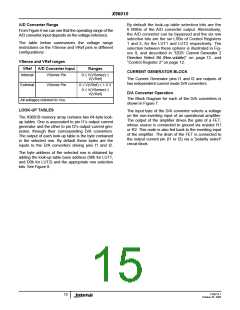
L1DAS D1DAS Control Source
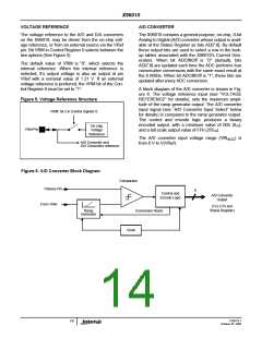
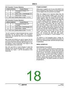
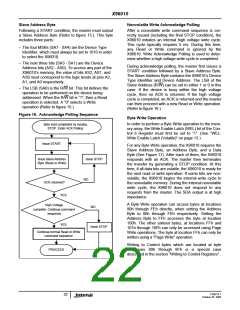
POWER-ON RESET
When power is applied to the Vcc pin of the X96010, the
device undergoes a strict sequence of events before the
current outputs of the D/A converters are enabled.
0
0
A/D converter through LUT1
(Default)
1
0
1
Bits L1DA5 - L1DA0 through LUT1
Bits D1DA7 - D1DA0
When the voltage at Vcc becomes larger than the
power-on reset threshold voltage (VPOR), the device
recalls all control bits from non-volatile memory into
volatile registers. Next, the analog circuits are pow-
ered up. When the voltage at Vcc becomes larger than
X
“X” = Don’t Care Condition (May be either “1” or “0”)
D/A Converter 2 Access Summary
a second voltage threshold (V
), the ADC is
ADCOK
enabled. In the default case, after the ADC performs
four consecutive conversions with the same exact
result, the ADC output is used to select a byte from
each look-up table. Those bytes become the input of
the DACs. During all the previous sequence the input
of both DACs are 00h. If bit ADCfiltOff is “1”, only one
ADC conversion is necessary. Bits D1DAS, D2DAS,
L1DAS, and L2DAS, also modify the way the two
DACs are accessed the first time after power-
uppower-up, as described in “Control Register 5” on
page 12.
L2DAS D2DAS
Control Source
0
0
A/D converter through LUT2
(Default)
1
0
1
Bits L2DA5 - L2DA0 through LUT2
Bits D2DA7 - D2DA0
X
“X” = Don’t Care Condition (May be either “1” or “0”)
The A/D converter is shared between the two current
generators but the look-up tables, D/A converters,
control bits, and selection bits can be set completely
independently.
The X96010 is a hot pluggable device. Voltage dis-
trubances on the Vcc pin are handled by the power-on
reset circuit, allowing proper operation during hot plug-
in applications.
Bits D1DAS and D2DAS are used to bypass the A/D
converter and look-up tables, allowing direct access to
the inputs of the D/A converters with the bytes in con-
trol registers 3 and 4 respectively. See Figure 8, and
the descriptions of the control bits.
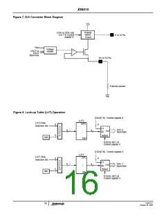
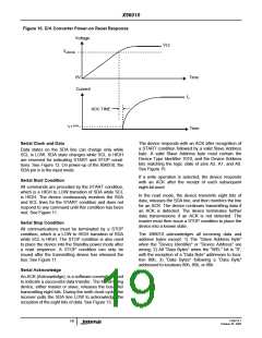
SERIAL INTERFACE
Bits I1DS and I2DS in Control Register 0 select the
direction of the currents through pins I1 and I2 inde-
pendently See Figure 7, and the descriptions of the
control bits.
Serial Interface Conventions
The device supports a bidirectional bus oriented proto-
col. The protocol defines any device that sends data
onto the bus as a transmitter, and the receiving device
as the receiver. The device controlling the transfer is
called the master and the device being controlled is
called the slave. The master always initiates data
transfers, and provides the clock for both transmit and
receive operations. The X96010 operates as a slave in
all applications.
FN8214.1
18
October 25, 2005

 INTERSIL [ Intersil ]