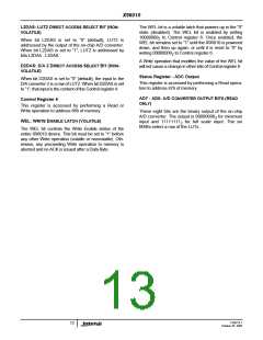
X96010
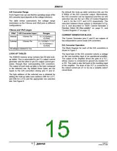
By examining the block diagram in Figure 7, we see
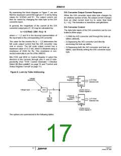
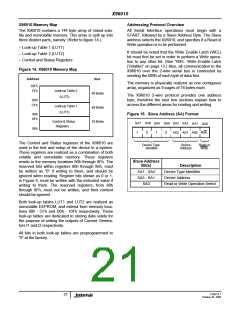
D/A Converter Output Current Response
that the maximum current through pin I1 is set by fixing
values for V(VRef) and R1. The output current can
then be varied by changing the data byte at the D/A
converter input.
When the D/A converter input data byte changes by
an arbitrary number of bits, the output current changes
from an intial current level (Ix) to some final level
(Ix + ∆Ix). The transition is monotonic and glitchless.
In general, the magnitude of the current at the D/A
converter output pins (I1, I2) may be calculated by:
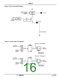
D/A Converter Control
The data byte inputs of the D/A converters can be con-
trolled in three ways:
Ix = (V(VRef) / (384 • Rx)) • N
where x = 1,2 and N is the decimal representation of
the input byte to the corresponding D/A converter.
– 1) With the A/D converter and through the look-up
tables (default),
The value for the resistor Rx (x = 1,2) determines the
full scale output current that the D/A converter may
sink or source. The full scale output current has a
maximum value of ±3.2 mA, which is obtained using a
resistance of 255Ω for Rx. This resistance is con-
nected externally to pin Rx of the X96010.
– 2) Bypassing the A/D converter and directly
accessing the look-up tables,
– 3) Bypassing both the A/D converter and look-up
tables, and directly setting the D/A converter input
byte.
Bits I1DS and I2DS in Control Register 0 select the
direction of the currents through pins I1 and I2 inde-
pendently (See “I1DS: Current Generator 1 Direction
Select Bit (Non-volatile)” on page 10 and “Control and
Status Register Format” on page 11).
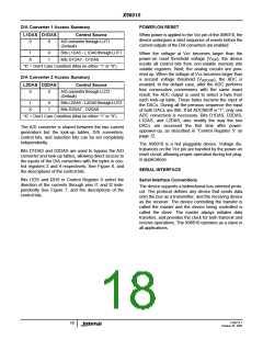
Figure 9. Look-Up Table Addressing
L2DA[5:0]:
Control
D1
Voltage
Reference
LUT2 Row
Selection bits
Register 2
Out
D0
Select
6
ADC
Voltage Input
L2DAS: bit 6 in
Control register 5
8
L1DA[5:0]:
Control
Register 1
6
D1
AD[7:0]
Status
Register
LUT1 Row
Selection bits
Out
D0
Select
L1DAS: bit 4 in
Control register 5
The options are summarized in the following tables:
FN8214.1
17
October 25, 2005

 INTERSIL [ Intersil ]