ISL6753
From the small signal current-mode model [1] it can be
shown that the naturally-sampled modulator gain, Fm,
without slope compensation, is
1
2
3
4
5
6
7
8
16
15
14
13
12
11
10
9
VIN
1
Fm = -------------------
(EQ. 9)
SnTsw
ISL6753
R3
C7
where Sn is the slope of the sawtooth signal and Tsw is the
duration of the half-cycle. When an external ramp is added,
the modulator gain becomes
RAMP
GND
1
1
(EQ. 10)
Fm = -------------------------------------- = ---------------------------
(Sn + Se)Tsw m SnTsw
c
where Se is slope of the external ramp and
Se
Sn
m
= 1 + -------
(EQ. 11)
c
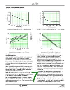
FIGURE 6. VOLTAGE FEED FORWARD CONTROL
The charging time of the ramp capacitor is
The criteria for determining the correct amount of external
ramp can be determined by appropriately setting the
damping factor of the double-pole located at half the
oscillator frequency. The double-pole will be critically
damped if the Q-factor is set to 1, and over-damped for Q >
1, and under-damped for Q < 1. An under-damped condition
can result in current loop instability.
V
RAMP(PEAK)
t = –R3 ⋅ C7 ⋅ ln 1 – ---------------------------------------
S
(EQ. 7)
V
IN(MIN)
For optimum performance, the maximum value of the
capacitor should be limited to 10nF. The maximum DC
current through the resistor should be limited to 2mA
maximum. For example, if the oscillator frequency is
400kHz, the minimum input voltage is 300V, and a 4.7nF
ramp capacitor is selected, the value of the resistor can be
determined by rearranging EQ. 7.
1
(EQ. 12
Q = -------------------------------------------------
π(m (1 – D) – 0.5)
c
where D is the percent of on time during a half cycle. Setting
Q = 1 and solving for Se yields
–6
–t
–2.5 ⋅ 10
R3 = ------------------------------------------------------------------------- = ------------------------------------------------------------
–9
1
300
V
RAMP(PEAK)
4.7 ⋅ 10 ⋅ ln 1 – ---------
C7 ⋅ ln 1 – ---------------------------------------
1
1
π
(EQ. 13)
-------------
S
= S
-- + 0.5
– 1
V
e
n
IN(MIN))
1 – D
= 159
kΩ
(EQ. 8)
Since Sn and Se are the on time slopes of the current ramp
and the external ramp, respectively, they can be multiplied
by Ton to obtain the voltage change that occurs during Ton.
where t is equal to the oscillator period minus the deadtime.
If the deadtime is short relative to the oscillator period, it can
be ignored for this calculation.
1
1
-------------
V
= V
-- + 0.5
– 1
(EQ. 14)
e
n
1 – D
π
If feed forward operation is not desired, the RC network may
be connected to VREF rather than the input voltage.
Alternatively, a resistor divider from CTBUF may be used as
the sawtooth signal. Regardless, a sawtooth waveform must
be generated on RAMP as it is required for proper PWM
operation.
where Vn is the change in the current feedback signal during
the on time and Ve is the voltage that must be added by the
external ramp.
Vn can be solved for in terms of input voltage, current
transducer components, and output inductance yielding
T
⋅ V ⋅ R
Slope Compensation
N
SW
CS
O
S
1
π
----------------------------------------- -------
V
=
⋅
-- + D – 0.5
V
(EQ. 15)
e
N
P
N
⋅ L
Peak current-mode control requires slope compensation to
improve noise immunity, particularly at lighter loads, and to
prevent current loop instability, particularly for duty cycles
greater than 50%. Slope compensation may be
CT
O
where R
is the current sense burden resistor, N is the
CT
CS
current transformer turns ratio, L is the output inductance,
O
accomplished by summing an external ramp with the current
feedback signal or by subtracting the external ramp from the
voltage feedback error signal. Adding the external ramp to
the current feedback signal is the more popular method.
V
is the output voltage, and Ns and Np are the secondary
O
and primary turns, respectively.
FN9182.1
10
March 10, 2005

 INTERSIL [ Intersil ]