ISL6753
The inductor current, when reflected through the isolation
transformer and the current sense transformer to obtain the
current feedback signal at the sense resistor yields
peak amplitude of CT (0.4 - 4.4V). A typical application sums
this signal with the current sense feedback and applies the
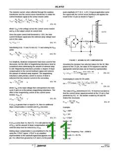
result to the CS pin as shown in Figure 7.
N
⋅ R
D ⋅ T
N
S
CS
SW
S
------------------------
--------------------
-------
V
=
I
+
V
⋅
– V
O
V
CS
O
IN
N
⋅ N
2L
O
N
P
1
P
CT
(EQ. 16)
2
3
4
5
6
7
8
CTBUF
where V
is the voltage across the current sense resistor
CS
and I is the output current at current limit.
O
ISL6753
R9
Since the peak current limit threshold is 1.00V, the total
current feedback signal plus the external ramp voltage must
sum to this value.
CS
V
+ V
= 1
CS
(EQ. 17)
e
R6
RCS
C4
Substituting EQs. 15 and 16 into EQ. 17 and solving for R
yields
CS
N
⋅ N
1
P
CT
----------------------- ------------------------------------------------------
R
=
⋅
Ω
(EQ. 18)
CS
N
V
O
S
1
D
-------
I
+
T
-- + ---
SW
π
O
L
2
O
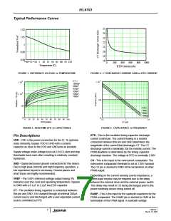
FIGURE 7. ADDING SLOPE COMPENSATION
For simplicity, idealized components have been used for this
discussion, but the effect of magnetizing inductance must be
considered when determining the amount of external ramp
to add. Magnetizing inductance provides a degree of slope
compensation to the current feedback signal and reduces
the amount of external ramp required. The magnetizing
inductance adds primary current in excess of what is
reflected from the inductor current in the secondary.
Assuming the designer has selected values for the RC filter
placed on the CS pin, the value of R9 required to add the
appropriate external ramp can be found by superposition.
(D(V
– 0.4) + 0.4) ⋅ R6
R6 + R9
CTBUF
(EQ. 22)
V
– ∆V
= ------------------------------------------------------------------------------
CS
V
e
Rearranging to solve for R9 yields
V
⋅ DT
IN
SW
(EQ. 19)
∆I = -------------------------------
A
(D(V
– 0.4) – V + ∆V
+ 0.4) ⋅ R6
CS
P
CTBUF
e
L
R9 = ------------------------------------------------------------------------------------------------------------------
– ∆V
Ω
m
V
e
CS
(EQ. 23)
where V is the input voltage that corresponds to the duty
IN
cycle D and Lm is the primary magnetizing inductance. The
effect of the magnetizing current at the current sense
The value of R
determined in EQ. 18 must be rescaled so
CS
that the current sense signal presented at the CS pin is that
predicted by EQ. 16. The divider created by R6 and R9
makes this necessary.
resistor, R , is
CS
∆I ⋅ R
P
CS
(EQ. 20)
∆V
= -------------------------
V
CS
N
CT
R6 + R9
----------------------
⋅ R
CS
(EQ. 24)
R′
=
CS
R9
If ∆V
CS
is greater than or equal to Ve, then no additional
slope compensation is needed and R
becomes
CS
Example:
N
CT
V
V
= 280V
R
= -------------------------------------------------------------------------------------------------------------------------------------
IN
CS
N
DT
N
V
⋅ DT
SW
S
SW
S
IN
-------
----------------
-------
⋅
I
+
⋅
V
⋅
– V
O
+ -------------------------------
= 12V
O
IN
O
N
P
2L
O
N
P
L
m
(EQ. 21)
L
= 2.0µH
O
Np/Ns = 20
Lm = 2mH
If ∆V is less than Ve, then EQ. 18 is still valid for the value
CS
of R , but the amount of slope compensation added by the
CS
external ramp must be reduced by ∆V
.
CS
I
= 55A
O
Adding slope compensation is accomplished in the ISL6753
using the CTBUF signal. CTBUF is an amplified
representation of the sawtooth signal that appears on the CT
pin. It is offset from ground by 0.4V and is 2x the peak-to-
Oscillator Frequency, Fsw = 400kHz
Duty Cycle, D = 85.7%
N
= 50
CT
FN9182.1
11
March 10, 2005

 INTERSIL [ Intersil ]