ISL6753
waveform is required at this input. For current-mode control
this pin is connected to CS and the current loop feedback
signal is applied to both inputs. For voltage-mode control,
the oscillator sawtooth waveform may be buffered and used
to generate an appropriate signal, RAMP may be connected
to the input voltage through a RC network for voltage feed
forward control, or RAMP may be connected to VREF
through a RC network to produce the desired sawtooth
waveform.
Functional Description
Features
The ISL6753 PWM is an excellent choice for low cost ZVS
full-bridge applications employing conventional output
rectification. If synchronous rectification is required, please
consider the ISL6752 or ISL6551 products.
With the ISL6753’s many protection and control features, a
highly flexible design with minimal external components is
possible. Among its many features are support for both
current- and voltage-mode control, a very accurate
overcurrent limit threshold, thermal protection, a buffered
sawtooth oscillator output suitable for slope compensation,
voltage controlled resonant delay, and adjustable frequency
with precise deadtime control.
OUTUL and OUTUR - These outputs control the upper
bridge FETs and operate at a fixed 50% duty cycle in
alternate sequence. OUTUL controls the upper left FET and
OUTUR controls the upper right FET. The left and right
designation may be switched as long as they are switched in
conjunction with the lower FET outputs, OUTLL and OUTLR.
Oscillator
RESDEL - Sets the resonant delay period between the
toggle of the upper FETs and the turn on of either of the
lower FETs. The voltage applied to RESDEL determines
when the upper FETs switch relative to a lower FET turning
on. Varying the control voltage from 0 to 2.00V increases the
resonant delay duration from 0 to 100% of the deadtime. The
control voltage divided by 2 represents the percent of the
deadtime equal to the resonant delay. In practice the
maximum resonant delay must be set lower than 2.00V to
ensure that the lower FETs, at maximum duty cycle, are OFF
prior to the switching of the upper FETs.
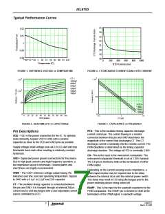
The ISL6753 has an oscillator with a programmable
frequency range to 2MHz, and can be programmed with an
external resistor and capacitor.
The switching period is the sum of the timing capacitor
charge and discharge durations. The charge duration is
determined by CT and a fixed 200µA internal current source.
The discharge duration is determined by RTD and CT.
3
T
≈ 11.5 ⋅ 10 ⋅ CT
S
(EQ. 1)
C
OUTLL and OUTLR - These outputs control the lower
bridge FETs, are pulse width modulated, and operate in
alternate sequence. OUTLL controls the lower left FET and
OUTLR controls the lower right FET. The left and right
designation may be switched as long as they are switched in
conjunction with the upper FET outputs, OUTUL and
OUTUR.
–9
(EQ. 2)
T
≈ (0.06 ⋅ RTD ⋅ CT) + 50 ⋅ 10
S
D
1
T
= T + T = ------------
S
(EQ. 3)
SW
C
D
F
SW
where T and T are the charge and discharge times,
C
D
VERR - The control voltage input to the inverting input of the
PWM comparator. The output of an external error amplifier
(EA) is applied to this input for closed loop regulation. VERR
has a nominal 1mA pull-up current source.
respectively, T
is the oscillator period, and F is the
SW
SW
oscillator frequency. One output switching cycle requires two
oscillator cycles. The actual times will be slightly longer than
calculated due to internal propagation delays of
approximately 10nS/transition. This delay adds directly to
the switching duration, but also causes overshoot of the
timing capacitor peak and valley voltage thresholds,
effectively increasing the peak-to-peak voltage on the timing
capacitor. Additionally, if very small discharge currents are
used, there will be increased error due to the input
impedance at the CT pin.
FB - FB is the inverting input to the error amplifier (EA).
SS - Connect the soft-start timing capacitor between this pin
and GND to control the duration of soft-start. The value of
the capacitor determines the rate of increase of the duty
cycle during start up.
SS may also be used to inhibit the outputs by grounding
through a small transistor in an open collector/drain
configuration.
The maximum duty cycle, D, and percent deadtime, DT, can
be calculated from:
CTBUF - CTBUF is the buffered output of the sawtooth
oscillator waveform present on CT and is capable of
sourcing 2mA. It is offset from ground by 0.40V and has a
nominal valley-to-peak gain of 2. It may be used for slope
compensation.
T
C
(EQ. 4)
D = ------------
T
SW
DT = 1 – D
(EQ. 5)
FN9182.1
8
March 10, 2005

 INTERSIL [ Intersil ]