ISL6753
To understand how the ZVS method operates one must
include the parasitic elements of the circuit and examine a
full switching cycle.
the node to VIN and then forward biases the body diode of
upper switch UR.
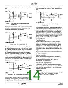
VIN+
UL
UR
VIN+
IS
D1
UL
UR
D1
VOUT+
RTN
LL
VOUT+
RTN
LL
IP
LL
LR
LL
LR
D2
D2
VIN-
VIN-
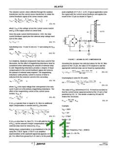
FIGURE 12. UL - UR FREE-WHEELING PERIOD
FIGURE 10. IDEALIZED FULL-BRIDGE
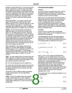
The primary leakage inductance, L , maintains the current
L
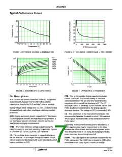
In Figure 10, the power semiconductor switches have been
replaced by ideal switch elements with parallel diodes and
capacitance, the output rectifiers are ideal, and the
which now circulates around the path of switch UL, the
transformer primary, and switch UR. When switch LR opens,
the output inductor current free-wheels through both output
diodes, D1 and D2. This condition persists through the
remainder of the half-cycle.
transformer leakage inductance has been included as a
discrete element. The parasitic capacitance has been
lumped together as switch capacitance, but represents all
parasitic capacitance in the circuit including winding
capacitance. Each switch is designated by its position, upper
left (UL), upper right (UR), lower left (LL), and lower right
(LR). The beginning of the cycle, shown in Figure 11, is
arbitrarily set as having switches UL and LR on and UR and
LL off. The direction of the primary and secondary currents
During the period when CT discharges, also referred to as
the deadtime, the upper switches toggle. Switch UL turns off
and switch UR turns on. The actual timing of the upper
switch toggle is dependent on RESDEL which sets the
resonant delay. The voltage applied to RESDEL determines
how far in advance the toggle occurs prior to a lower switch
turning on. The ZVS transition occurs after the upper
switches toggle and before the diagonal lower switch turns
on. The required resonant delay is 1/4 of the period of the LC
resonant frequency of the circuit formed by the leakage
inductance and the parasitic capacitance. The resonant
transition may be estimated from EQ. 27.
are indicated by I and I , respectively.
P
S
VIN+
UL
LL
UR
LR
IS
D1
VOUT+
RTN
LL
IP
π
2
1
-------------------------------------
τ =
(EQ. 27)
2
1
R
-------------- – ---------
2
L
L C
D2
L
P
4L
VIN-
where τ is the resonant transition time, L is the leakage
L
FIGURE 11. UL - LR POWER TRANSFER CYCLE
inductance, C is the parasitic capacitance, and R is the
P
equivalent resistance in series with L and C .
L
P
The UL - LR power transfer period terminates when switch
LR turns off as determined by the PWM. The current flowing
in the primary cannot be interrupted instantaneously, so it
must find an alternate path. The current flows into the
parasitic switch capacitance of LR and UR which charges
The resonant delay is always less than or equal to the
deadtime and may be calculated using the following
equation.
V
resdel
2
-------------------
τ
=
⋅ DT
S
(EQ. 28)
resdel
where τ
resdel
is the desired resonant delay, V
voltage between 0 and 2V applied to the RESDEL pin, and
DT is the deadtime (see EQs. 1 - 5).
is a
resdel
When the upper switches toggle, the primary current that
was flowing through UL must find an alternate path. It
charges/discharges the parasitic capacitance of switches UL
and LL until the body diode of LL is forward biased. If
FN9182.1
13
March 10, 2005

 INTERSIL [ Intersil ]