ISL6753
R6 = 499Ω
Solve for the current sense resistor, R , using EQ. 18.
Using CT to provide slope compensation instead of CTBUF
requires the same calculations, except that EQs. 21 and 22
require modification. EQ. 21 becomes:
CS
R
= 15.1Ω.
CS
2D ⋅ R6
R6 + R9
V
– ∆V
= ----------------------
CS
V
(EQ. 25)
e
Determine the amount of voltage, Ve, that must be added to
the current feedback signal using EQ. 15.
and EQ. 22 becomes:
Ve = 153mV
(2D – V + ∆V ) ⋅ R6
e
CS
(EQ. 26)
R9 = ------------------------------------------------------------
– ∆V
Ω
Next, determine the effect of the magnetizing current from
EQ. 20.
V
e
CS
The buffer transistor used to create the external ramp from
CT should have a sufficiently high gain so as to minimize the
required base current. Whatever base current is required
reduces the charging current into CT and will reduce the
oscillator frequency.
∆V
CS
= 91mV
Using EQ. 23, solve for the summing resistor, R9, from
CTBUF to CS.
R9 = 30.1kΩ
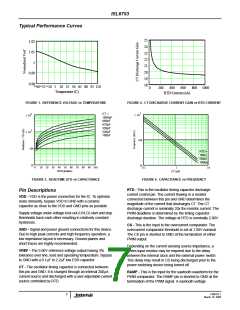
ZVS Full-Bridge Operation
Determine the new value of R , R’ , using EQ. 24.
CS CS
The ISL6753 is a full-bridge zero-voltage switching (ZVS)
PWM controller that behaves much like a traditional hard-
switched topology controller. Rather than drive the diagonal
bridge switches simultaneously, the upper switches (OUTUL,
OUTUR) are driven at a fixed 50% duty cycle and the lower
switches (OUTLL, OUTLR) are pulse width modulated on
the trailing edge.
R’
CS
= 15.4Ω
The above discussion determines the minimum external
ramp that is required. Additional slope compensation may be
considered for design margin.
f the application requires deadtime less than about 500nS,
the CTBUF signal may not perform adequately for slope
compensation. CTBUF lags the CT sawtooth waveform by
300-400nS. This behavior results in a non-zero value of
CTBUF when the next half-cycle begins when the deadtime
is short.
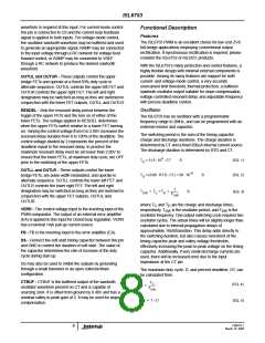
CT
DEADTIME
Under these situations, slope compensation may be added
by externally buffering the CT signal as shown below.
PWM
PWM
OUTLL
OUTLR
OUTUR
PWM
PWM
1
2
3
4
5
6
7
8
VREF 16
15
14
13
12
11
10
9
RESONANT
DELAY
ISL6753
OUTUL
RESDEL
WINDOW
CT
CS
R9
FIGURE 9. BRIDGE DRIVE SIGNAL TIMING
R6
RCS
C4
CT
FIGURE 8. ADDING SLOPE COMPENSATION USING CT
FN9182.1
12
March 10, 2005

 INTERSIL [ Intersil ]