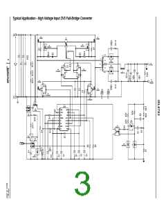
ISL6753
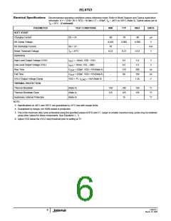
Typical Performance Curves
25
24
23
22
21
20
19
18
1.02
1.01
1
0.99
0.98
40 25 10 5 20 35 50 65 80 95 110
0
200
400
600
800 1000
Temperature (C)
RTD Current (uA)
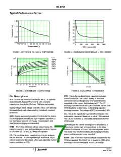
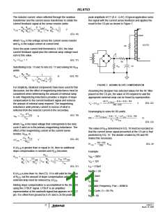
FIGURE 1. REFERENCE VOLTAGE vs TEMPERATURE
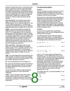
FIGURE 2. CT DISCHARGE CURRENT GAIN vs RTD CURRENT
3
.
4
CT =
.
1 10
1 10
1000pF
680pF
470pF
330pF
220pF
100pF
3
.
1 10
100
100
10
RTD=
10k
Ω
50k
Ω
100k
Ω
10
0
10 20 30 40 50 60 70 80 90 100
RTD (kohms)
0.1
1
10
CT (nF)
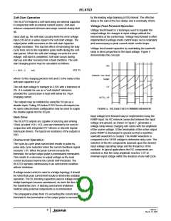
FIGURE 3. DEADTIME (DT) vs CAPACITANCE
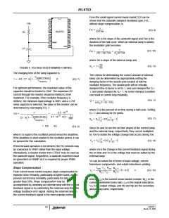
FIGURE 4. CAPACITANCE vs FREQUENCY
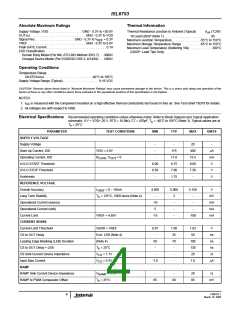
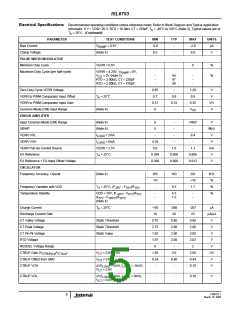
RTD - This is the oscillator timing capacitor discharge
current control pin. The current flowing in a resistor
connected between this pin and GND determines the
magnitude of the current that discharges CT. The CT
discharge current is nominally 20x the resistor current. The
PWM deadtime is determined by the timing capacitor
discharge duration. The voltage at RTD is nominally 2.00V.
Pin Descriptions
VDD - VDD is the power connection for the IC. To optimize
noise immunity, bypass VDD to GND with a ceramic
capacitor as close to the VDD and GND pins as possible.
Supply voltage under-voltage lock-out (UVLO) start and stop
thresholds track each other resulting in relatively constant
hysteresis.
CS - This is the input to the overcurrent comparator. The
overcurrent comparator threshold is set at 1.00V nominal.
The CS pin is shorted to GND at the termination of either
PWM output.
GND - Signal and power ground connections for this device.
Due to high peak currents and high frequency operation, a
low impedance layout is necessary. Ground planes and
short traces are highly recommended.
Depending on the current sensing source impedance, a
series input resistor may be required due to the delay
between the internal clock and the external power switch.
This delay may result in CS being discharged prior to the
power switching device being turned off.
VREF - The 5.00V reference voltage output having 3%
tolerance over line, load and operating temperature. Bypass
to GND with a 0.1µF to 2.2µF low ESR capacitor.
CT - The oscillator timing capacitor is connected between
this pin and GND. It is charged through an internal 200µA
current source and discharged with a user adjustable current
source controlled by RTD.
RAMP - This is the input for the sawtooth waveform for the
PWM comparator. The RAMP pin is shorted to GND at the
termination of the PWM signal. A sawtooth voltage
FN9182.1
7
March 10, 2005

 INTERSIL [ Intersil ]