ISL6366
to adjust R
ISEN
balance between all channels.
two or more times to achieve optimal thermal
output-voltage deviation is less than the allowable maximum.
Neglecting the contribution of inductor current and regulator
response, the output voltage initially deviates by an amount, as
shown in Equation 45:
Load-Line Regulation Resistor
The load-line regulation resistor is labelled R in Figure 14. Its
value depends on the desired loadline requirement of the
application.
di
dt
(EQ. 45)
FB
ΔV ≈ (ESL) ---- + (ESR) ΔI
The filter capacitor must have sufficiently low ESL and ESR so
that ΔV < ΔV
.
MAX
The desired loadline can be calculated using Equation 42:
V
Most capacitor solutions rely on a mixture of high-frequency
capacitors with relatively low capacitance in combination with
bulk capacitors having high capacitance but limited high-
frequency performance. Minimizing the ESL of the high-
frequency capacitors allows them to support the output voltage
as the current increases. Minimizing the ESR of the bulk
capacitors allows them to supply the increased current with less
output voltage deviation.
DROOP
R
= ------------------------
(EQ. 42)
LL
I
FL
where I is the full load current of the specific application, and
FL
DROOP
condition.
VR
is the desired voltage droop under the full load
Based on the desired loadline R , the loadline regulation
LL
resistor can be calculated using Equation 43:
⋅ R
The ESR of the bulk capacitors also creates the majority of the
output-voltage ripple. As the bulk capacitors sink and source the
inductor AC ripple current (see “Interleaving” on page 14 and
Equation 2), a voltage develops across the bulk-capacitor ESR
N ⋅ R
LL
ISEN
R
X
R
= --------------------------------------
(EQ. 43)
FB
where N is the active channel number, R
ISEN
is the sense resistor
connected to the ISEN+ pin, and R is the resistance of the
equal to I
(ESR). Thus, once the output capacitors are
X
C,PP
selected, the maximum allowable ripple voltage, V
current sense element, either the DCR of the inductor or R
,
SEN
PP(MAX)
depending on the sensing method.
determines the lower limit on the inductance, as shown in
Equation 46.
If one or more of the current sense resistors are adjusted for
thermal balance (as in Equation 41), the load-line regulation
resistor should be selected based on the average value of the
current sensing resistors, as given in Equation 44:
V
⋅ K
OUT
RCM
(EQ. 46)
L
---------------------------------------------------------
≥ ESR ⋅
F
⋅ V ⋅ V
IN
SW
PP(MAX)
R
LL
Since the capacitors are supplying a decreasing portion of the
load current while the regulator recovers from the transient, the
capacitor voltage becomes slightly depleted. The output
inductors must be capable of assuming the entire load current
R
= ---------
R
ISEN(n)
(EQ. 44)
∑
FB
R
X
n
where R
ISEN(n)
is the current sensing resistor connected to the
th
n
ISEN+ pin.
before the output voltage decreases more than ΔV
. This
MAX
places an upper limit on inductance.
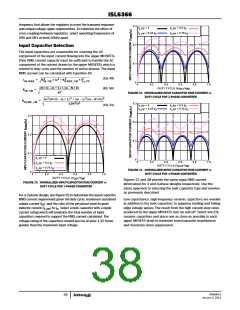
Output Filter Design
Equation 47 gives the upper limit on L for the cases when the
trailing edge of the current transient causes a greater output-
voltage deviation than the leading edge. Equation 48 addresses
the leading edge. Normally, the trailing edge dictates the
selection of L because duty cycles are usually less than 50%.
Nevertheless, both inequalities should be evaluated, and L
should be selected based on the lower of the two results. In each
equation, L is the per-channel inductance, C is the total output
capacitance, and N is the number of active channels.
The output inductors and the output capacitor bank together to
form a low-pass filter responsible for smoothing the pulsating
voltage at the phase nodes. The output filter also must provide
the transient energy until the regulator can respond. Because it
has a low bandwidth compared to the switching frequency, the
output filter necessarily limits the system transient response. The
output capacitor must supply or sink load current while the
current in the output inductors increases or decreases to meet
the demand.
2 ⋅ N ⋅ C ⋅ V
OUT
(EQ. 47)
L ≤ --------------------------------------- ΔV
– ΔI ⋅ ESR
MAX
In high-speed converters, the output capacitor bank is usually the
most costly (and often the largest) part of the circuit. Output filter
design begins with minimizing the cost of this part of the circuit.
The critical load parameters in choosing the output capacitors are
the maximum size of the load step, ΔI; the load-current slew rate,
di/dt; and the maximum allowable output-voltage deviation under
2
(
)
ΔI
(EQ. 48)
⋅ N ⋅ C
1.25
⎛
⎝
⎞
L ≤ ---------------------------- ΔV
– ΔI ⋅ ESR
V
– V
IN OUT
MAX
2
⎠
(
)
ΔI
Switching Frequency Selection
transient loading, ΔV
. Capacitors are characterized according
MAX
There are a number of variables to consider when choosing the
switching frequency, as there are considerable effects on the upper-
MOSFET loss calculation. These effects are outlined in “MOSFETs”
on page 35, and they establish the upper limit for the switching
frequency. The lower limit is established by the requirement for fast
transient response and small output-voltage ripple as outlined in
“Output Filter Design” on page 37. Choose the lowest switching
to their capacitance, ESR, and ESL (equivalent series inductance).
At the beginning of the load transient, the output capacitors supply
all of the transient current. The output voltage will initially deviate by
an amount approximated by the voltage drop across the ESL. As the
load current increases, the voltage drop across the ESR increases
linearly until the load current reaches its final value. The capacitors
selected must have sufficiently low ESL and ESR so that the total
FN6964.0
January 3, 2011
37

 INTERSIL [ Intersil ]