ISL6366
.
TABLE 12. TIE-HIGH AND TIE-LOW OPTIONS (Continued)
I
= I
C
DVC
R
FBS
REG
R
R
DATA
UP
DW
VOUT
I
C
IMAXS
I
RC
C
R
(R
:
FSS_DRPS
0C
0E
ADDR
BT (R
GND/VCC)
TMAX
R
C
C
C
I
DVC
C
R
DVC
DVC
:
FS_DRP
GND/VCC)
FB
DVC
COMP
FDVID
10mV/µs
20mV/µs
10mV/µs
20mV/µs
DE
TCOMP
29.7°C
1.1V/1.05V
1.1V/1.05V
0
OPEN 10kΩ 00h
x1.333
-
29.7°C 10kΩ OPEN 1Fh
29.7°C OPEN 499kΩ C0h
+
ERROR
AMPLIFIER
0
29.7°C 499kΩ OPEN DFh
V
DAC
I
+I
ISL6366 INTERNAL CIRCUIT
RC DROOP_ACTUAL
0F
NPSI
IMAX
SI1/CI1
SI1/CI1
SI2/CI2
SI2/CI2
ENABLED
ENABLED
190A
255A
190A
255A
OPEN 10kΩ 00h
10kΩ OPEN 1Fh
OPEN 499kΩ C0h
499kΩ OPEN DFh
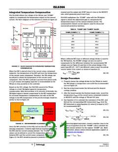
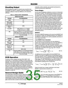
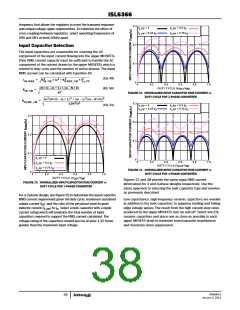
FIGURE 28. DYNAMIC VID COMPENSATION NETWORK
The amount of compensation current required is dependant on
the modulator gain of the system, K1, and the error amplifier R-C
DISABLED
DISABLED
components, R and C , that are in series between the FB and
C
C
COMP pins. Use Equations 26, 27, and 28 to calculate the RC
component values, R and C , for the VID-on-the-fly
NOTE: Whenever 10kΩ is tie-high or tie-low, 0Ω can be used.
DVC
DVC
compensation network. For these equations: V is the input
IN
is the oscillator ramp
voltage for the power train; V
RAMP
amplitude as in Equation 3; and R and C are the error amplifier
Dynamic VID Compensation (DVC)
C
C
During a VID transition, the resulting change in voltage on the FB pin
and the COMP pin causes an AC current to flow through the error
amplifier compensation components from the FB to the COMP pin.
R-C components between the FB and COMP pins.
V
(EQ. 26)
IN
-----------------
K1 =
V
RAMP
This current then flows through the feedback resistor, R , and can
FB
K1
cause the output voltage to overshoot or undershoot at the end of
the VID transition. In order to ensure the smooth transition of the
output voltage during a VID change, a VID-on-the-fly compensation
network is required. This network is composed of a resistor and
R
= A ⋅ R
-----------------------------
(EQ. 27)
(EQ. 28)
A =
DVC
C
3 ⋅ (K1 – 1)
C
C
A
------
C
=
DVC
capacitor in series, R
and C , between the DVC and the FB pin.
DVC
DVC
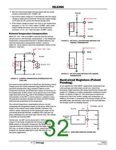
During DVID transitions, extra current builds up in the output
capacitors due to the C*dv/dt. The current is sensed by the
controller and fed across the feedback resistor creating extra
droop (if enabled) and causing the output voltage not properly
tracking the DAC voltage. Placing a series R-C to ground from the
FB pin can sink this extra DVID induced current.
This VID-on-the-fly compensation network works by sourcing AC
current into the FB node to offset the effects of the AC current
flowing from the FB to the COMP pin during a VID transition. To
create this compensation current, the controllers set the voltage
on the DVC pin to be 4/3 of the voltage on the DAC. Since the
error amplifier forces the voltage on the FB pin and the DAC to be
equal, the resulting voltage across the series RC between DVC
and FB is equal to the DAC voltage. The RC compensation
C
⋅ R
OUT
R
LL
(EQ. 29)
---------------------------
C =
FB
C
⋅ R
LL
C
components, R
and C , can then be selected to create the
OUT
DVC
DVC
(EQ. 30)
---------------------------
R =
= R
FB
desired amount of compensation current.
When the output voltage overshoots during DVID, the RDVC-CDVC
network can be used to compensate the movement of the
error-amplifier compensation network. When the output voltage
is lagging from DAC (or SVALERT#) or having a rough-off prior to
the final settling of DVID, the R-C network can be used to
compensate for the extra droop current generated by the
C*dv/dt. Sometimes, both networks can work together to
achieve the best result. In such case, both networks need to be
fine tuned in the board level for optimized performance.
FN6964.0
January 3, 2011
34

 INTERSIL [ Intersil ]