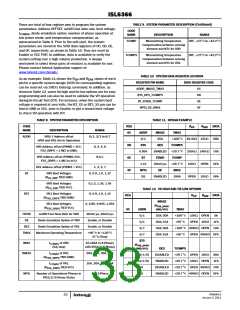
ISL6366
TABLE 9. SYSTEM PARAMETER DESCRIPTION (Continued)
There are total of four register pins to program the system
parameters: Address OFFSET, setVID fast slew rate, boot voltage,
, diode emulation option, number of phase operation at
CODE
I
CCMAX
NAME
DESCRIPTION
RANGE
low power mode, and temperature compensation, as
summarized in Table 9. Prior to the soft-start, the system
parameters are stored in the SVID data registers of 0C, 0D, 0E,
and 0F, respectively, as shown in Table 10. They are reset by
Enable or VCC POR. In addition, data is available to verify the
system setting over a high volume production. A design
worksheet to select these pairs of resistors is available for use.
Please contact Intersil Application support at
TCOMP
Mismatching Temperature
Compensation between sensing
element and NTC for VR0
OFF, +13°C to +43.2°C
TCOMPS
Mismatching Temperature
Compensation between sensing
element and NTC for VR1
OFF, +13°C to +43.2°C
www.intersil.com/design/.
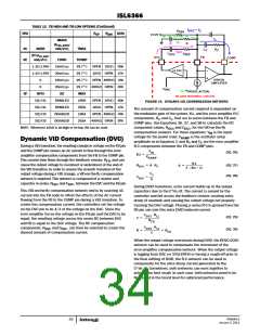
TABLE 10. SYSTEM DATA REGISTER LOCATION
As an example, Table 11 shows the R and R
UP DW
values of each
REGISTER PIN NAME
ADDR_IMAXS_TMAX
BTS_DES_TCOMPS
BT_FDVID_TCOMP
NPSI_DE_IMAX
DATA REGISTER CODE
pin for a specific system design; DATA for corresponding registers
can be read out via SVID’s Get(reg) command. In addition, as
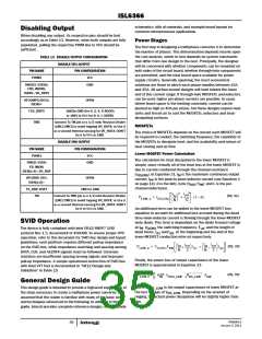
shown in Table 12, some tie-high and tie-low options are for easy
programming and can also be used to validate the VR operation
during In-Circuit Test (ICT). For instance, when the system boot
voltage is required at zero Volts, the BT_XX or BTS_XX pin can be
tied to GND or VCC, prior to Enable, to get a known boot voltage
to check VR operation with ICT.
0C
0D
0E
0F
TABLE 9. SYSTEM PARAMETER DESCRIPTION
TABLE 11. DESIGN EXAMPLE
CODE
REG
0C
R
R
DATA
08h
UP
DW
NAME
ADDR
DESCRIPTION
RANGE
ADDR
0/1
IMAXS
25A
TMAX
VR0/1 Address offset
(VR0 and VR1 Are In Operation)
0/1, 2/3 to 6/7
+100°C 29.4kΩ 15kΩ
0D
0E
0F
BTS
DES
TCOMPS
VR0 Address offset (PWMS = VCC,
0, 2, 4, 6
8,A,C
FSS_DRPS = 1 MΩ to GND)
0.85V
BT
ENABLED +29.7°C 255kΩ 140kΩ C0h
FDVID TCOMP
20mV/µs +29.7°C
VR0 Address offset (PWMS=VCC,
FSS_DRPS = 1 MΩ to VCC)
1.1V
NPSI
SI1
10kΩ
OPEN
DFh
VR1 Address offset (PWM1 = VCC)
1, 3, 5, 7
DE
IMAX
190A
BT
VR0 Boot Voltages
0, 0.9, 1.0, 1.1V
ENABLED
OPEN
10kΩ
00h
(R
TIED GND)
FS_DRP
VR0 Boot Voltages
(R TIED VCC)
0,1.2, 1.35, 1.5V
0, 0.9, 1.0, 1.1V
FS_DRP
VR1 Boot Voltages
(R TIED GND)
TABLE 12. TIE-HIGH AND TIE-LOW OPTIONS
BTS
REG
0C
R
R
DATA
0h
UP
DW
FSS_DRPS
VR1 Boot Voltages
(R TIED VCC)
IMAXS
0, 0.85, 0.925, 1.05V
(R
:
FSS_DRPS
FSS_DRPS
ADDR
0/1
GND/VCC)
35A/30A
20A/15A
35A/30A
20A/15A
TMAX
+100°C 10kΩ OPEN
+95°C
+100°C 499kΩ OPEN C0h
FDVID
DE
setVID Fast Slew Rate for VR0
Diode Emulation Option of VR0
Diode Emulation Option of VR1
Maximum Operating Temperature
10mV/µs, 20mV/µs
Enable, or Disable
Enable, or Disable
0/1
OPEN 10kΩ 1Fh
DES
6/7
TMAX
+90°C to +120°C
(5°C/Step)
6/7
+95°C
OPEN 499kΩ DFh
BTS
IMAX
I
I
of VR0
(5A/step)
15-165A (1:4-Phase);
105-255A (5:6-Phase)
CCMAX
CCMAX
(R
:
FSS_DRPS
GND/VCC)
0D
DES
TCOMPS
IMAXS
of VR1
TIED GND)
20A, 25A, 30A, 35A
15A, 20A, 25A, 30A
1 or 2-Phase
1.1V/1.5V
DISABLED
ENABLED
DISABLED
ENABLED
+29.7°C OPEN 10kΩ 00h
+29.7°C 10kΩ OPEN 1Fh
+29.7°C OPEN 499kΩ C0h
+29.7°C 499kΩ OPEN DFh
(R
(R
FSS_DRPS
1.1V/1.5V
I
of VR1
TIED VCC)
CCMAX
0
0
FSS_DRPS
NPSI
Number of Operational Phases in
PSI1/2/3/Decay States
FN6964.0
January 3, 2011
33

 INTERSIL [ Intersil ]