ISL6366
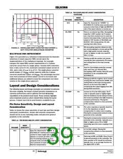
TABLE 14. PIN DESIGN AND/OR LAYOUT CONSIDERATION
0.6
0.4
0.2
0
(Continued)
NOISE
PIN NAME
NC5
SENSITIVITY
DESCRIPTION
No
Open Pin. Reserved for “ISENIN+” in
ISL6366A/67: It will be noise sensitive and
connects to the Drain of High-side MOSFET
side of the input inductor or resistor pin.
EN_PWR
No
There is an internal 1µs filter. Decoupling
capacitor is NOT needed, but if needed,
use a low time constant one to avoid too
much of shut-down delay. It will also be the
output of CFP function in ISL6366A and
ISL6367: 34Ω strong pull-up. 25 mils
spacing from other traces.
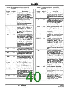
I
I
I
= 0
= 0.5 I
= 0.75 I
L,PP
L,PP
L,PP
O
O
0
0.2
0.4
0.6
0.8
1.0
DUTY CYCLE (V
/V
)
OUT IN
RAMP_ADJ
Yes
NO decoupling capacitor allowed on this
pin, but decoupling its resistor pull-up RAIL
with a high quality ceramic capacitor
(0.1µF or higher) or with very small RC
filter (<2.2µs).
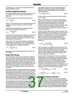
FIGURE 32. NORMALIZED INPUT-CAPACITOR RMS CURRENT vs
DUTY CYCLE FOR SINGLE-PHASE CONVERTER
MULTIPHASE RMS IMPROVEMENT
Figure 32 is provided as a reference to demonstrate the dramatic
reductions in input-capacitor RMS current upon the
implementation of the multiphase topology. For example,
compare the input RMS current requirements of a 2-phase
converter versus that of a single phase. Assume both converters
have a duty cycle of 0.25, maximum sustained output current of
RGND
VSEN
Yes
No
Pairing up with the positive rail remote
sensing line that connected to FB resistor,
and routing them to the load sensing
points.
Used for Overvoltage protection sensing
only, and it has 1µs internal filter.
Decoupling is NOT needed. Add a 0Ω series
impedance to be compatible with
ISL6366A/67.
40A, and a ratio of I
would require 17.3A
to I of 0.5. The single phase converter
current capacity while the 2-phase
L,PP
RMS
O
converter would only require 10.9A
. The advantages become
RMS
even more pronounced when output current is increased and
additional phases are added to keep the component cost down
relative to the single phase approach.
FB
Yes
Yes
Pairing up with the negative rail of remote
sensing line that connected to RGND, and
routing them to the load sensing points.
Reserve an RC from FB to GND to
compensate the output lagging from DAC
during DVID transitions.
Layout and Design Considerations
The following layout and design strategies are intended to minimize
the noise coupling, the impact of board parasitic impedances on
converter performance and to optimize the heat-dissipating
capabilities of the printed-circuit board. These sections highlight
some important practices which should follow during the layout
process. A layout check list in excel format is available for use.
HFCOMP
Connect an R to the VR0 output. The R
value is typically equal or slightly higher
than the feedback resistor (droop resistor),
fine tuned according to the high frequency
transient performance. Placing the
compensation network in close proximity
to the controller.
Pin Noise Sensitivity, Design and Layout
Consideration
Table 14 shows the noise sensitivity of each pin and their design
and layout consideration. All pins and external components
should not be across switching nodes and placed in general
proximity to the controller.
PSICOMP
COMP
Yes
Yes
The series impedance typically should be
2x-3x the impedance in type III
compensation to reduce noise coupling.
Placing the compensation network in close
proximity to the controller.
Placing the compensation network in close
proximity to the controller. Typically use a
68pF or higher across FB to COMP
depending upon the noise coupling of the
layout.
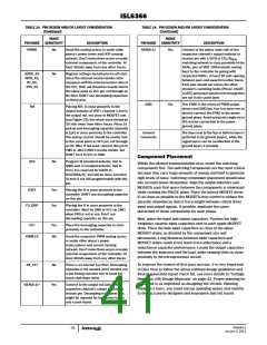
TABLE 14. PIN DESIGN AND/OR LAYOUT CONSIDERATION
NOISE
PIN NAME SENSITIVITY
NC4 No
DESCRIPTION
DVC
Yes
Yes
4/3 of DAC voltage. Placing the
compensation network in close proximity
to the controller.
Open Pin. Reserved for “ISENIN-” in
ISL6366A/67: It will be noise sensitive and
connect to input supply side of the input
inductor or resistor pin with L/DCR or
ESL/R matching network in close
proximity to the controller. Place NTC in the
close proximity to input inductor for
thermal compensation.
IMON
Referring to GND, not RGND. Place R and C
in general proximity to the controller. The
time constant of RC should be sufficient,
typically 1ms, as an average function for
the digital IOUT of VR0.
FN6964.0
January 3, 2011
39

 INTERSIL [ Intersil ]