ISL6366
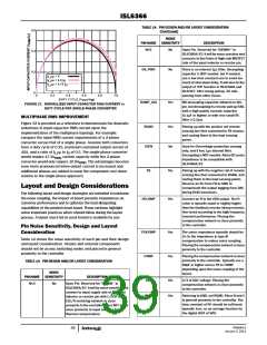
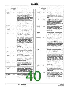
TABLE 14. PIN DESIGN AND/OR LAYOUT CONSIDERATION
(Continued)
TABLE 14. PIN DESIGN AND/OR LAYOUT CONSIDERATION
(Continued)
NOISE
NOISE
PIN NAME SENSITIVITY
DESCRIPTION
PIN NAME
COMPS
SENSITIVITY
DESCRIPTION
SVDATA;
SVCLK
Yes
13 to 26MHz signals when the SVID bus is
sending commands, pairing up with
SVALERT# and routing carefully back to
CPU socket. 20 mils spacing within
SVDATA, SVALERT#, and SVCLK; and more
than 30 mils to all other signals. Refer to
the Intel individual platform design
guidelines and place proper terminated
(pull-up) resistance for impedance
matching. Local decoupling capacitor is
needed for the pull-up rail.
Yes
Yes
Placing the compensation network in close
proximity to the controller. Typically use a
68pF or higher across FBS to COMPS
depending upon the noise coupling of the
layout.
FBS
Pairing up with the negative rail of remote
sensing line that connected to RGNDS, and
routing them to the load sensing points.
Reserve an RC from FBS to GND to
compensate the output lagging from DAC
during DVID transitions.
SVALERT#
VR_RDY
NC3
No
No
No
Open drain and high dv/dt pin during
transitions. Routing it in the middle of
SVDATA and SVCLK. Also see above.
VSENS
No
Used for Overvoltage protection sensing
only, and it has 1µs internal filter.
Decoupling is NOT needed. Add a series
impedance to be compatible with
ISL6366A/67.
Open drain and high dv/dt pin. Avoid its
pull-up higher than VCC. Tie it to ground
when not used.
RGNDS
Pairing up with the positive rail remote
sensing line that connected to FB resistor,
and routing them to the load sensing
points.
Floating Pins. Reserved pull-up resistors
2
for I C/PMBus in ISL6367A: I2CLK pin, it
will be noise sensitive. 100kHz to 2MHz
2
signal when the I C or PMBus is sending
FSS_DDRS
Yes
Placing the R in close proximity to the
controller. Avoid using decoupling
capacitor on this pin. Must tie GND or VCC
via 1MΩ depending upon the desired
ADDRESS offset when VR1 is not in use.
Don’t use decoupling capacitor on this pin.
To minimize the effect of cross coupling
between regulators, select operating
frequencies of VR0 and VR1 at least 50kHz
apart.
commands, pairing up with PMALERT#
and routing carefully back to PMBus. 20
mils spacing within I2DATA, PMALERT#,
and I2CLK; and more than 30 mils to all
other signals. Refer to the PMBus design
guidelines and place proper terminated
(pull-up) resistance for impedance
matching.
NC1
NC2
No
No
Floating Pins. Reserved pull-up resistors
2
for I C/PMBus in ISL6367: I2DATA pin, it
TMS
Placing NTC in close proximity to the
output inductor of VR1 and to the output
rail, not close to MOSFET side (see
will be noise sensitive. Also see above.
Floating Pins. Reserved pull-up resistors
for PMBus in ISL6367: PMALERT# pin.
Also see above.
Figure 23); the return trace should be 25
mils away from other traces. Place 1k pull-
up and decoupling capacitor (typically
0.1µF) in close proximity to the controller.
The pull-up resistor should be exactly tied
to the same point as VCC pin, not through
an RC filter. If not used, connect this pin to
TM or 1MΩ/2MΩ resistor divider, but
DON’T tie it to VCC or GND. Place the NTC
in proximity to the output rail, not close to
MOSFET side.
IMONS
Yes
Referring to GND, not RGNDS. Place R and
C in general proximity to the controller. The
time constant of RC should be sufficient,
typically 1ms, as an average function for
the digital IOUT of VR1.
VR_HOT#
No
Open drain and high dv/dt pin during
transitions. Avoid its pull-up rail higher
than VCC. 30 mils spacing from other
traces.
ISENS+
ISENS-
Yes
Yes
Connect to the output rail side of the
output inductor or current sensing resistor
HFCOMPS/D
VCS
Yes
Connect an R in similar value (equal or
slight higher) of the feedback resistor. If
programmed to be used as DVCS, Connect
an RC to FBS from this pin. Placing the
compensation network in close proximity
to the controller.
pin with I
resistor and decoupling
SEN
capacitor (27ns) placed in close proximity
to the controller.
Connect to the phase node side of the
output inductor or resistor pin with L/DCR
or ESL/R
matching network in close
VR_RDYS
No
Open drain and high dv/dt pin. Avoid its
pull-up higher than VCC. Tie it to GND when
not used.
SEN
proximity to the ISENS± pins of the
controller. Differential pair with ISENS+
routing back to the controller.
FN6964.0
January 3, 2011
40

 INTERSIL [ Intersil ]