ISL6366
schematics, bills of materials, and example board layouts for
common microprocessor applications.
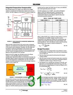
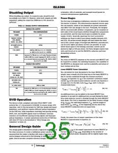
Disabling Output
When disabling any output, its respective pins should be tied
accordingly as in Table 13. However, when both outputs are fully
populated, pulling the respective PWM line to VCC should be
sufficient.
Power Stages
The first step in designing a multiphase converter is to determine
the number of phases. This determination depends heavily upon
the cost analysis, which in turn depends on system constraints
that differ from one design to the next. Principally, the designer
will be concerned with whether components can be mounted on
both sides of the circuit board; whether through-hole components
are permitted; and the total board space available for power
supply circuitry. Generally speaking, the most economical
solutions are those in which each phase handles between 15A
and 25A. All surface-mount designs will tend toward the lower
end of this current range. If through-hole MOSFETs and inductors
can be used, higher per-phase currents are possible. In cases
where board space is the limiting constraint, current can be
pushed as high as 40A per phase, but these designs require heat
sinks and forced air to cool the MOSFETs, inductors and heat-
dissipating surfaces.
TABLE 13. DISABLE OUTPUT CONFIGURATION
DISABLE VR1 OUTPUT
PIN NAME
PWMS
PIN CONFIGURATION
VCC
RNGDS; VSENS;
FBS; IMONS;
ISENS-; VR_RDYS
GND
HFCOMPS/DVCS;
ISENS+
OPEN
FSS_DRPS
1MΩto GND (for 0, 2, 4, 6 ADDR)
or 1MΩ to VCC for 8, A, C ADDR)
TMS
Connect To TM pin or a 1/2 ratio Resistor Divider
(1MΩ/2MΩ) to avoid tripping VR_HOT#; or Use it
as a second thermal sensing for VR_HOT#. DON’T
tie it to VCC or GND.
MOSFETs
The choice of MOSFETs depends on the current each MOSFET will
be required to conduct; the switching frequency; the capability of
the MOSFETs to dissipate heat; and the availability and nature of
heat sinking and air flow.
DISABLE VR0 OUTPUT
PIN NAME
PWM1
PIN CONFIGURATION
Lower MOSFET Power Calculation
VCC
The calculation for heat dissipated in the lower MOSFET is
simple, since virtually all of the heat loss in the lower MOSFET is
due to current conducted through the channel resistance
RNGD; VSEN;
FB; IMON;
ISEN[1:4]-; VR_RDY
GND
(r
). In Equation 31, I is the maximum continuous output
DS(ON)
M
HFCOMP; DVC;
ISEN[1:6]+
OPEN
current; I is the peak-to-peak inductor current (see Equation 1
PP
on page 14); d is the duty cycle (V
/V ); and L is the per-
OUT IN
channel inductance.
FS_DRP, RSET
TM
1MΩ to GND
2
2
I
⎛
⎜
⎝
⎞
⎟
⎠
I
PP
Connect To TMS pin or a 1/2 ratio Resistor Divider
(1MΩ/2MΩ) to avoid tripping VR_HOT#; or Use it
as a second thermal sensing for VR_HOT#. DON’T
tie it to VCC or GND.
(EQ. 31)
M
P
= r
+ --------- ⋅ (1 – d)
12
-----
LOW, 1
DS(ON)
N
An additional term can be added to the lower-MOSFET loss
equation to account for additional loss accrued during the dead
time when inductor current is flowing through the lower-MOSFET
body diode. This term is dependent on the diode forward voltage
SVID Operation
at I , V
; the switching frequency, F ; and the length of
The device is fully compliant with Intel VR12/IMVP7 SVID
protocol Rev 1.5, document# of 456098. To ensure proper CPU
operation, refer to this document for SVID bus design and layout
guidelines; each platform requires different pull-up impedance
on the SVID bus, while impedance matching and spacing among
DATA, CLK, and ALERT# signals must be followed. Common
mistakes are insufficient spacing among signals and improper
pull-up impedance. A simple operational instruction of SVID bus
with Intel VTT Tool is documented in “VR12 Design and
Validation” in Table 15.
M
D(ON)
sw
dead times, t and t , at the beginning and the end of the
d1 d2
lower-MOSFET conduction interval respectively.
⎛
⎞
⎟
⎠
I
I
M
I
I
⎛
⎝
⎞
⎠
M
PP
PP
2
(EQ. 32)
(EQ. 33)
P
= V
F
D(ON) SW
t
t
d2
+ ⎜
--------
----- –
----- + --------
LOW, 2
d1
N
2
⎝ N
Finally, the power loss of output capacitance of the lower
MOSFET is approximated in Equation 33:
2
3
1.5
--
P
≈
⋅ V
⋅ C
⋅
V
⋅ F
DS_LOW SW
LOW,3
IN
OSS_LOW
General Design Guide
where C
is the output capacitance of lower MOSFET at
This design guide is intended to provide a high-level explanation of
the steps necessary to create a multiphase power converter. It is
assumed that the reader is familiar with many of the basic skills
and techniques referenced in the following. In addition to this
guide, Intersil provides complete reference designs, which include
OSS_LOW
the test voltage of V
. Depending on the amount of
DS_LOW
ringing, the actual power dissipation will be slightly higher than
this.
FN6964.0
January 3, 2011
35

 INTERSIL [ Intersil ]