ISL6227
Voltage Monitor and Protections
The converter output is monitored and protected against
extreme overload, short circuit, overvoltage, and
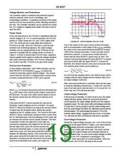
PGOOD
VOUT
1
2
8 CLK
IL
undervoltage conditions. A sustained overload on the output
SHUTDOWN
sets the PGOOD low and latches off the offending channel of
the chip. The controller operation can be restored by cycling
the VCC voltage or toggling both enable (EN) pins to low to
clear the latch.
3
Power Good
In the soft-start process, the PGOOD is established after the
soft pin voltage is at 1.5V. In normal operation, the PGOOD
window is 100mV below the 0.9V and 135mV higher than
0.9V. The VSEN pin has to stay within this window for
PGOOD to be high. Since the VSEN pin is used for both
feedback and monitoring purposes, the output voltage
deviation can be coupled directly to the VSEN pin by the
capacitor in parallel with the voltage divider as shown in
Figure 4. In order to prevent false PGOOD drop, capacitors
need to parallel at the output to confine the voltage deviation
with severe load step transient. The PGOOD comparator
has a built-in 3µs filter. PGOOD is an open drain output.
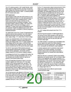
µ
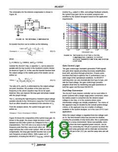
Ch1 5.0V
Ch3 1.0A
Ch2 100mV
M 10.0 s
Ω
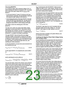
FIGURE 40. OVERCURRENT PROTECTION
Due to the nature of the used current sensing technique,
and to accommodate a wide range of the r
variation,
DS(ON)
the value of the overcurrent threshold should set at about
180% of the nominal load value. If more accurate current
protection is desired, a current sense resistor placed in
series with the lower MOSFET source may be used. The
inductor current going through the lower MOSFET is sensed
and held at 400ns after the upper MOSFET is turned off;
therefore, the sensed current is very close to its peak value.
The inductor peak current can be written as:
Overcurrent Protection
In dual switcher application, both PWM controllers use the
(V – V ) • V
IN
o
o
(EQ.16)
I
= ------------------------------------------- + I
load
lower MOSFETs on-resistance r
to monitor the
peak
DS(ON),
2L • F
• V
IN
o
SW
current for protection against shorted outputs. The sensed
current from the ISEN pin is compared with a current set by
a resistor connected from the OCSET pin to ground:
As seen from the equation above, the inductor peak current
changes with the input voltage and the inductor value once
an output voltage is selected.
10.3V
R
= --------------------------------------------------------
(EQ.15)
SET
I
• r
DS(ON)
After overcurrent protection is activated, there are two ways
to bring the offending channel back: (1) Both EN1 and EN2
have to be held low to clear the latch, (2) To recycle the Vcc
of the chip, the POR will clear the latch.
OC
-------------------------------------- + 8µA
R
+ 140Ω
CS
where, I
CS
is a desired overcurrent protection threshold and
OC
R
is the value of the current sense resistor connected to
Undervoltage Protection
the ISEN pin. The 8µA is the offset current added on top of
the sensed current from the ISEN pin for internal circuit
biasing.
In the process of operation, if a short circuit occurs, the output
voltage will drop quickly. Before the overcurrent protection
circuit responds, the output voltage will fall out of the required
regulation range. The chip comes with undervoltage protection.
If a load step is strong enough to pull the output voltage lower
than the undervoltage threshold, the offending channel latches
off immediately. The undervoltage threshold is 75% of the
nominal output voltage. Toggling both pins to low, or recycling
Vcc, will clear the latch and bring the chip back to operation.
If the lower MOSFET current exceeds the overcurrent
threshold, a pulse skipping circuit is activated. The upper
MOSFET will not be turned on as long as the sensed current
is higher than the threshold value, limiting the current
supplied by the DC voltage source. The current in the lower
MOSFET will be continuously monitored until it is lower than
the OC threshold value, then the following UGATE pulse will
be released and normal current sample resumes. This kind
of operation remains for eight clock cycles after the
Overvoltage Protection
Should the output voltage increase over 115% of the normal
value due to the upper MOSFET failure, or for other reasons,
the overvoltage protection comparator will force the
synchronous rectifier gate driver high. This action actively
pulls down the output voltage and eventually attempts to
blow the battery fuse. As soon as the output voltage is within
regulation, the OVP comparator is disengaged. The
MOSFET driver will restore its normal operation. When the
OVP occurs, the PGOOD will drop to low as well.
overcurrent comparator was tripped for the first time. If after
the first eight clock cycles the current exceeds the
overcurrent threshold again, in a time interval of another
eight clock cycles, the overcurrent protection latches and
disables the offending channel. If the overcurrent condition
goes away during the first eight clock cycles, normal
operation is restored and the overcurrent circuit resets itself
at the end of sixteenth clock cycles; see Figure 40.
19

 INTERSIL [ Intersil ]