ISL6227
This OVP scheme provides a ‘soft’ crowbar function, which
helps clamp the voltage overshoot, and does not invert the
output voltage when otherwise activated with a continuously
high output from lower MOSFET driver - a common problem
for OVP schemes with a latch.
For the VTT channel where output is derived from the VDDQ
output, some control and protective functions have been
significantly simplified. For example, the overcurrent, and
overvoltage, and undervoltage protections for the second
channel controller are disabled when the DDR pin is set
high. The hysteretic mode of operation is also disabled on
the VTT channel to allow sinking capability to be
DDR Application
High throughput Double Data Rate (DDR) memory ICs are
replacing traditional memory ICs in the latest generation of
Notebook PCs and in other computing devices. A novel
feature associated with this type of memory are the
referencing and data bus termination techniques. These
techniques employ a reference voltage, VREF, that tracks
the center point of VDDQ and VSS voltages, and an
additional VTT power source where all terminating resistors
are connected. Despite the additional power source, the
overall memory power consumption is reduced compared to
traditional termination.
independent from the load level. As the VTT channel tracks
the VDDQ/2 voltage, the soft-start function is not required,
and the SOFT2 pin may be left open, in the event both
channels are enabled simultaneously. However, if the VTT
channel is enabled later than the VDDQ, the SOFT2 pin
must have a capacitor in place to ensure soft-start. In case of
overcurrent or undervoltage caused by short circuit on VTT,
the fault current will propagate to the first channel and shut
down the converter.
The VREF voltage will be present even if the VTT is
disabled.
The added power source has a cluster of requirements that
should be observed and considered. Due to the reduced
differential thresholds of DDR memory, the termination
power supply voltage, VTT, closely tracks VDDQ/2 voltage.
Channel Synchronization in DDR Applications
The presence of two PWM controllers on the same die
requires channel synchronization, to reduce inter-channel
interference that may cause the duty factor jitter and
increased output ripple.
Another very important feature of the termination power
supply is the capability to operate at equal efficiency in
sourcing and sinking modes. The VTT supply regulates the
output voltage with the same degree of precision when
current is flowing from the supply to the load, and when the
current is diverted back from the load into the power supply.
The PWM controller is at greatest noise susceptibility when
an error signal on the input of the PWM comparator
approaches the decision making point. False triggering may
occur, causing jitter and affecting the output regulation.
The ISL6227 dual channel PWM controller possesses
several important enhancements that allow re-configuration
for DDR memory applications, and provides all three
voltages required in a DDR memory compliant computer.
A common approach used to synchronize dual channel
converters is out-of-phase operation. Out-of-phase
operation reduces input current ripple and provides a
minimum interference for channels that control different
voltage levels.
To reconfigure the ISL6227 for a complete DDR solution, the
DDR pin should be set high permanently to the VCC rail.
This activates some functions inside the chip that are
specific to DDR memory power needs.
When the DDR pin is connected to GND for dual switcher
applications, the channels operate 180° out-of-phase. When
used in a DDR application with cascaded converters (VTT
generated from VDDQ), several methods of synchronization
are implemented in the ISL6227. In the DDR mode, when
the DDR pin is connected to VCC, the channels operate
either with 0° phase shift, when the VIN pin is connected to
the GND, or with 90° phase shift if the VIN pin is connected
to a voltage higher than 4.2V.
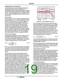
In the DDR application presented in Figure 32, the first
controller regulates the VDDQ rail to 2.5V. The output
voltage is set by external dividers Rfb1 and Rfb12. The
second controller regulates the VTT rail to VDDQ/2. The
OCSET2 pin function is now different, and serves as an
input that brings VDDQ/2 voltage, created by the Rd1 and
Rd2 divider, inside the chip, effectively providing a tracking
function for the VTT voltage.
The following table lists the different synchronization
schemes and their usage:
The PG2 pin function is also different in DDR mode. This pin
becomes the output of the buffer, whose input is connected
to the center point of the R/R divider from the VDDQ output
by the OCSET2 pin. The buffer output voltage serves as a
1.25V reference for the DDR memory chips. Current
capability of this pin is 10mA (12mA max).
DDR PIN
VIN PIN
Vin pin >4.2V
SYNCHRONIZATION
180° out of phase
0° phase
0
1
1
Vin pin voltage <4.2V
Vin pin voltage >4.2V
90° phase shift
20

 INTERSIL [ Intersil ]