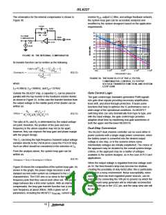
ISL6227
and the change the current loop gain. The lower the current
sensing resistor, the higher gain of the current loop, which
can damp the output LC filter more.
Application Information
Design Procedures
GENERAL
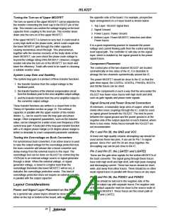
A ceramic decoupling capacitor should be used between the
VCC and GND pin of the chip. There are three major
currents drawn from the decoupling capacitor:
A higher value current-sensing resistor will decrease the
current sense gain. If the phase node of the converter is very
noisy due to poor layout, the sensed current will be
contaminated, resulting in duty cycle jittering by the current
loop. In such a case, a bigger current sense resistor can be
used to reduce both real and noise current levels. This can
help damp the phase node wave form jittering.
1. the quiescent current, supporting the internal logic and
normal operation of the IC
2. the gate driver current for the lower MOSFETs
Sometimes, if the phase node is very noisy, a resistor can be
put on the ISEN pin to ground. This resistor together with the
3. and the current going through the external diodes to the
bootstrap capacitor for upper MOSFET.
R
can divide the phase node voltage down, seen by the
CS
In order to reduce the noisy effect of the bootstrap capacitor
current to the IC, a small resistor, such as 10Ω, can be used
with the decoupling cap to construct a low pass filter for the
IC, as shown in Figure 41. The soft-start capacitor and the
resistor divider setting the output voltage is easy to select as
discussed in the “Block Diagram” on page 13.
internal current sense amplifier, and reduce noise coupling.
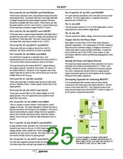
Sizing the Overcurrent Setpoint Resistor
The internal 0.9V reference is buffered to the OCSET pin
with a voltage follower (refer to the equivalent circuit in
Figure 42). The current going through the external
overcurrent set resistor is sensed from the OCSET pin. This
current, divided by 2.9, sets up the overcurrent threshold and
compares with the scaled ISEN pin current going through
TO BOOT
VCC
5V
R
with an 8µA offset. Once the sensed current is higher
CS
10Ω
than the threshold value, an OC signal is generated. The first
OC signal starts a counter and activates a pulse skipping
function. The inductor current will be continuously monitored
through the phase node voltage after the first OC trip. As
long as the sensed current exceeds the OC threshold value,
the following PWM pulse will be skipped. This operation will
be the same for 8 switching cycles. Another OC occurring
between 8 to 16 switching cycles would result in a latch off
with both upper and lower drives low. If there is no OC within
8 to 16 switching cycles, normal operation resumes.
FIGURE 41. INPUT FILTERING FOR THE CHIP
Selection of the Current Sense Resistor
The value of the current sense resistor determines the gain
of the current sensing circuit. It affects the current loop gain
and the overcurrent protection setpoint. The voltage drop on
the lower MOSFET is sensed within 400ns after the upper
MOSFET is turned off. The current sense pin has a 140Ω
resistor in series with the external current sensing resistor.
The current sense pin can source up to a 260µA current
while sensing current on the lower MOSFET, in such a way
that the voltage drop on the current sensing path would be
equal to the voltage on the MOSFET.
ISEN
140 Ω
PHASE
RCS
_
+
_
8uA
+
+
Σ
Rdson
+
÷ 33.1
I
(R + 140Ω) = I r
(EQ.17)
SOURCING CS
D DS(ON)
Isense
OCSET
_
+
+
_
OC
0.9 V
Reference
I
can be assumed to be the inductor peak current. In a
Amplifier
D
Comparator
Rset
worst case scenario, the high temperature r
DS(ON)
could
÷ 2.9
increase to 150% of the room temperature level. During
overload condition, the MOSFET drain current I could be
D
130% higher than the normal inductor peak. If the inductor
has 30% peak-to-peak ripple, I would equal to 115% of the
FIGURE 42. EQUIVALENT CIRCUIT FOR OC SIGNAL
GENERATOR
D
load current. The design should consider the above factors
so that the maximum I
will not saturate to 260µA
should
SOURCING
Based on the above description and functional block
diagram, the OC set resistor can be calculated as:
under worst case conditions. To be safe, I
SOURCING
be less than 100µA in normal operation at room
10.3V
temperature. The formula in the earlier discussion assumes
a 75µA sourcing current. Users can tune the sourcing
current of the ISEN pin to meet the overcurrent protection
R
= ---------------------------------------------------
set
I
r
(EQ.18)
OC DS(ON)
-------------------------------- + 8µA
+ 140
R
CS
21

 INTERSIL [ Intersil ]