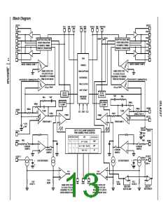
ISL6227
The resistor connected to the ISEN pin sets the gain in the
current sensing. The following expression estimates the
required value of the current sense resistor, depending on
the maximum continuous load current, and the value of the
TABLE 2. PWM COMPARATOR RAMP VOLTAGE AMPLITUDE
FOR DDR APPLICATION
VRAMP
VIN PIN CONNECTION
AMPLITUDE
MOSFETs r
current.
, assuming the ISEN pin sources 75µA
DS(ON)
Ch1
Input Voltage
Input voltage >4.2V
Input voltage <4.2V
Vin/8
1.25V
I
• r
MAX
DS(ON)
(EQ. 6)
R
= ------------------------------------------ – 140Ω
75µA
CS
GND
1.25V
Ch2
Input voltage >4.2V
GND
0.625V
1.25V
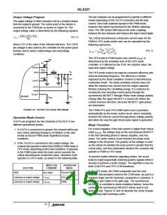
Because the current sensing circuit is a sample-and-hold
type, the information obtained at the last moment of the
sampling is used. This current sensing circuit samples the
inductor current very close to its peak value. The current
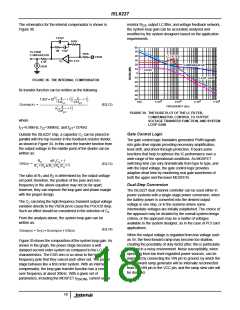
The small signal transfer function from the error amplifier
feedback essentially injects a resistor R in series with the
output voltage V to the output voltage V can be written in
i
c
o
original LC filter as shown in Figure 37, where the sample-
and-hold effect of the current loop has been ignored. Vc and
Vo are small signal components extracted from its DC
operation points.
the following expression:
s
-------- + 1
R
o
Wz
(EQ. 8)
--------------------------------------- ---------------------------------------------------------
G(s) = G
m
R + DCR + R
s
s
o
------------ + 1 ------------ + 1
i
Wp1
Wp2
Ri
Lo
DCR
+
The dc gain is derived by shorting the inductor and opening
the capacitor. There is one zero and two poles in this transfer
function. The zero is related to ESR and the output
capacitor.
Co
ESR
+
Gm*Vc
Ro
Vo
-
-
The first pole is a low frequency pole associated with the
output capacitor and its charging resistors. The inductor can
be regarded as short. The second pole is the high frequency
pole related to the inductor. At high frequency the output
capacitor can be regarded as a short circuit. By
approximation, the poles and zero are inversely proportional
to the time constants, associated with inductor and capacitor,
by the following expressions:
FIGURE 37. THE EQUIVALENT CIRCUIT OF THE POWER
STAGE WITH CURRENT LOOP INCLUDED
The value of the injected resistor can be estimated by:
V
r
R
IN
DS(ON)
(EQ. 7)
--------------------------------------------
• 4.4kΩ
R
=
i
V
+ 140
ramp CS
R is in kΩ, and R
DS
and R are in Ω . V divided by
CS IN
i
1
Wz = -----------------------
(EQ. 9)
V
, is defined as Gm, which is a constant 8 or 18 dB for
ESR*C
o
ramp
both channels in dual switcher applications, when V is
IN
above 3V. Refer to Table 1 for the ramp amplitude in different
1
Wp1 = ------------------------------------------------------------------------------
(EQ.10)
||
V
pin connections. The feed-forward effect of the V is
(ESR + (R + DCR) R )*C
IN
IN
i
o
o
reflected in Gm. V is defined as the error amplifier output
c
voltage.
||
R + DCR + ESR
R
o
(EQ.11)
i
Wp2 = ----------------------------------------------------------
L
o
TABLE 1. PWM COMPARATOR RAMP AMPLITUDE FOR
DUAL SWITCHER APPLICATION
Since the current loop separates the LC resonant poles into
two distant poles, and ESR zero tends to cancel the high
frequency pole, the second order system behaves like a first
order system. This control method simplifies the design of
the internal compensator and makes it possible to
accommodate many applications having a wide range of
parameters.
VRAMP
VIN PIN CONNECTIONS
Ch1 and Ch2 Input Voltage Input voltage >4.2V
Input voltage <4.2V
AMPLITUDE
Vin/8
1.25V
GND
1.25V
17

 INTERSIL [ Intersil ]