ISL6227
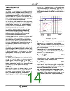
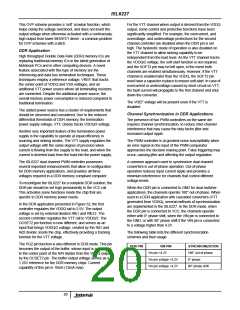
waiting for the transition to occur. The transition decision
VOUT
IIND
point is aligned with the PWM clock. When the need for
transition is detected, there is a 500ns delay between the
first/last pulse of the PWM controller from the last/first pulse
of the hysteretic mode controller.
t
t
Current Sensing
PHASE
COMP
The current on the lower MOSFET is sensed by measuring
its voltage drop within its on-time. In order to activate the
current sampling circuitry, two conditions need to be met.
(1) the Lgate is high and (2) the phase pin sees a negative
voltage for regular buck operation, which means the current
is freewheeling through lower MOSFET. For the second
channel of the DDR application, the phase pin voltage needs
to be higher than 0.1V to activate the current sensing circuit
for bidirectional current sensing. The current sampling
finishes at about 400ns after the lower MOSFET has turned
on. This current information is held for current mode control
and overcurrent protection. The current sensing pin can
source up to 260µA. The current sense resistor and OCSET
resistor can be adjusted simultaneously for the same
overcurrent protection level, however, the current sensing
gain will be changed only according to the current sense
resistor value, which will affect the current feedback loop
gain. The middle point of the Isen current can be at 75µA,
but it can be tuned up and down to fit application needs.
t
t
1
2
3
4 5
6 7 8
Hysteretic
MODE
PWM
OF
OPERATION
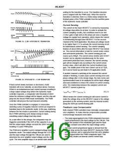
FIGURE 35. CCM—HYSTERETIC TRANSITION
VOUT
IIND
t
t
1
2
3
4 5
6
7
8
PHASE
COMP
t
t
Hysteretic
MODE
OF
OPERATION
PWM
If another channel is switching at the moment the current
sample is finishing, it could cause current sensing error and
phase voltage jitter. In the design stage, the duty cycles and
synchronization have to be analyzed for all the input voltage
and load conditions to reduce the chance of current sensing
error. The relationship between the sampled current and
MOSFET current is given by:
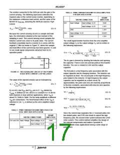
FIGURE 36. HYSTERETIC—CCM TRANSITION
If load current slowly increases or decreases, mode
transition will occur naturally, as described above; however,
if there is an instantaneous load current increase resulting in
a large output voltage drop before the hysteretic mode
controller responds, a comparator with threshold of 20mV
below the reference voltage will be tripped, and the chip will
jump into the forced PWM mode immediately. The PWM
controller will process the load transient smoothly.
I
(R
+ 140)= r
I
DS(ON) D
(EQ. 5)
SEN CS
Which means the current sensing pin will source current to
make the voltage drop on the MOSFET equal to the voltage
generated on the sensing resistor, plus the internal resistor,
along the ISEN pin current flowing path.
Once the PWM controller is engaged, 8 consecutive
switching cycles of negative inductor current are required to
transition back to the hysteretic mode. In this way, chattering
between the two modes is prevented. Current sinking during
the 8 PWM switching cycle dumps energy to input,
smoothing output voltage load step-down.
Feedback Loop Compensation
Both channel PWM controllers have internally compensated
error amplifiers. To make internal compensation possible
several design measures were taken.
• The ramp signal applied to the PWM comparator has been
made proportional to the input voltage by the VIN pin. This
keeps the product of the modulator gain and the input
voltage constant even when the input voltage varies.
As a side effect to this design, the comparator may be
triggered consistently if the ESR of the capacitor is so big
that the output ripple voltage exceeds the 20mV window,
resulting in a pure PWM pulse.
• The load current proportional signal is derived from the
voltage drop across the lower MOSFET during the PWM
off time interval, and is subtracted from the error amplifier
output signal before the PWM comparator input. This
effectively creates an internal current control loop.
The PWM error amplifier is put in clamped voltage during the
hysteretic mode. The output voltage through the VOUT pin
and the input voltage through the VIN pin are used to
determine the error amplifier output voltage and the duty
cycle. The error amplifier stays in an armed state while
16

 INTERSIL [ Intersil ]