ISL6227
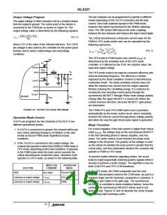
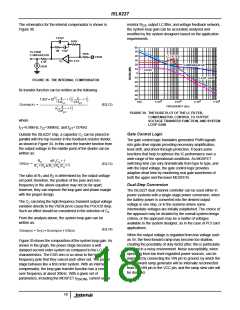
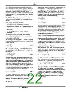
The schematics for the internal compensator is shown in
Figure 38.
resistor R , output LC filter, and voltage feedback network,
CS
the system loop gain can be accurately analyzed and
modified by the system designers based on the application
requirements.
1.25pF
500K
60
50
40
30
20
10
1M 15pF
TO PWM
300K
COMPARATOR
LC FILTER
VSEN
-
+
0.9V
Vc
4.4K
COMPENSATOR
ISEN
VO/VC
0
-10
-20
-30
-40
-50
-60
LOOP GAIN
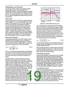
FIGURE 38. THE INTERNAL COMPENSATOR
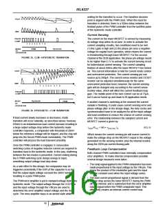
Its transfer function can be written as the following:
5
s
s
1.857 • 10 -------------- + 1 -------------- + 1
3
4
5
6
2πf
2πf
100
1•10
1•10
FREQUENCY (Hz)
1•10
1•10
z1
z2
Gcomp(s) = --------------------------------------------------------------------------------------------
(EQ.12)
s
2πf
s --------------- + 1
p1
FIGURE 39. THE BODE PLOT OF THE LC FILTER,
COMPENSATOR, CONTROL TO OUTPUT
where
VOLTAGE TRANSFER FUNCTION, AND SYSTEM
LOOP GAIN
f
=6.98kHz, f =380kHz, and f =137kHz
z1 z2 p1
Gate Control Logic
Outside the ISL6227 chip, a capacitor C can be placed in
z
parallel with the top resistor in the feedback resistor divider,
as shown in Figure 34. In this case the transfer function from
the output voltage to the middle point of the divider can be
written as:
The gate control logic translates generated PWM signals
into gate drive signals providing necessary amplification,
level shift, and shoot-through protection. It bears some
functions that help to optimize the IC performance over a
wide range of the operational conditions. As MOSFET
switching time can vary dramatically from type to type, and
with the input voltage, the gate control logic provides
adaptive dead time by monitoring real gate waveforms of
both the upper and the lower MOSFETs.
R
sR C + 1
1 z
2
-----------------------------------------------------------------
Gfd(s) =
(EQ.13)
||
R
+ R s(R R )C + 1
1
2
1
2
z
The ratio of R and R is determined by the output voltage
1
2
set point; therefore, the position of the pole and zero
frequency in the above equation may not be far apart;
however, they can improve the loop gain and phase margin
with the proper design.
Dual-Step Conversion
The ISL6227 dual channel controller can be used either in
power systems with a single-stage power conversion, when
the battery power is converted into the desired output
voltage in one step, or in the systems where some
intermediate voltages are initially established. The choice of
the approach may be dictated by the overall system design
criteria, or the approach may be a matter of voltages
available to the system designer, as in the case of PCI card
applications.
The C can bring the high frequency transient output voltage
z
variation directly to the VSEN pin to cause the PGOOD drop.
Such an effect should be considered in the selection of C .
z
From the analysis above, the system loop gain can be
written as:
(EQ.14)
Gloop(s) = G(s) • Gcomp(s) • Gfd(s)
When the output voltage is regulated from low voltage such
as 5V, the feed-forward ramp may become too shallow,
creating the possibility of duty-factor jitter; this is particularly
relevant in a noisy environment. Noise susceptibility, when
operating from low level regulated power sources, can be
improved by connecting the VIN pin to ground, by which the
feed-forward ramp generator will be internally reconnected
from the VIN pin to the VCC pin, and the ramp slew rate will
be doubled.
Figure 39 shows the composition of the system loop gain. As
shown in the graph, the power stage becomes a well
damped second order system as compared to the LC filter
characteristics. The ESR zero is so close to the high
frequency pole that they cancel each other out. The power
stage behaves like a first order system. With an internal
compensator, the loop gain transfer function has a cross
over frequency at about 30kHz. With a given set of
parameters, including the MOSFET r
, current sense
DS(ON)
18

 INTERSIL [ Intersil ]