HSP50110
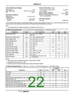
Absolute Maximum Ratings
Thermal Information (Typical)
o
Supply Voltage . . . . . . . . . . . . . . . . . . . . . . . . . . . . . . . . . . . . +7.0V
Input, Output Voltage . . . . . . . . . . . . . . . . .GND -0.5V to V +0.5V
ESD . . . . . . . . . . . . . . . . . . . . . . . . . . . . . . . . . . . . . . . . . . . .Class 3
Thermal Resistance (Typical, Note 3)
θ
( C/W)
JA
CC
PLCC Package. . . . . . . . . . . . . . . . . . . . . . . . . . . . .
23
o
Maximum Junction Temperature . . . . . . . . . . . . . . . . . . . . . . .150 C
o
o
Maximum Storage Temperature. . . . . . . . . . . . . . . . -65 C to 150 C
Maximum Lead Temperature (Soldering 10s) . . . . . . . . . . . . .300 C
o
Operating Conditions
(PLCC - Lead Tips Only)
Voltage Range . . . . . . . . . . . . . . . . . . . . . . . . . . . .+4.75V to +5.25V
Temperature Range
o
o
Die Characteristics
Commercial . . . . . . . . . . . . . . . . . . . . . . . . . . . . . . . . 0 C to 70 C
o
o
Industrial. . . . . . . . . . . . . . . . . . . . . . . . . . . . . . . . . -40 C to 85 C
Gate Count . . . . . . . . . . . . . . . . . . . . . . . . . . . . . . . . . 38,000 Gates
CAUTION: Stresses above those listed in “Absolute Maximum Ratings” may cause permanent damage to the device. This is a stress only rating and operation of the
device at these or any other conditions above those indicated in the operational sections of this specification is not implied.
NOTE:
3. θ is measured with the component mounted on an evaluation PC board in free air.
JA
o
o
o
o
DC Electrical Specifications
PARAMETER
V
= 5.0V ±5%, T = 0 to 70 C Commercial, T = -40 to 85 C Industrial
CC
A
A
SYMBOL
TEST CONDITIONS
MIN
MAX
UNITS
Power Supply Current
I
V
= Max, CLK = 52.6MHz
-
350
mA
CCOP
CC
Notes 4, 5
Standby Power Supply Current
Input Leakage Current
Output Leakage Current
Clock Input High
I
V
V
V
V
V
V
V
= Max, Outputs Not Loaded
-
-10
-10
3.0
-
500
10
10
-
µA
µA
V
CCSB
CC
CC
CC
CC
CC
CC
CC
I
= Max, Input = 0V or V
= Max, Input = 0V or V
= Max, CLK
I
CC
I
O
CC
V
V
IHC
Clock Input Low
V
= Min, CLK
0.8
-
V
ILC
Logical One Input Voltage
Logical Zero Input Voltage
Logical One Output Voltage
Logical Zero Output Voltage
Input Capacitance
V
= Max
2.0
-
V
IH
V
= Min
0.8
-
V
IL
V
I
I
= -400µA, V
= Min
2.6
-
V
OH
OH
OL
CC
V
= 2mA, V
CC
= Min
0.4
10
10
V
OL
C
CLK = 1MHz
All measurements referenced to GND.
-
pF
pF
IN
Output Capacitance
C
-
o
OUT
T
= 25 C, Note 6
A
NOTES:
4. Power supply current is proportional to frequency. Typical rating is 7mA/MHz.
5. Output load per test circuit and C = 40pF.
L
6. Not tested, but characterized at initial design and at major process/design changes.
o
o
o
o
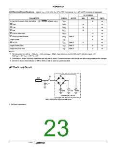
AC Electrical Specifications Note 8, V = 5.0V ±5%, T = 0 to 70 C Commercial, T = -40 to 85 C Industrial
CC
A
A
-52 (52.6MHz)
PARAMETER
SYMBOL
NOTES
MIN
MAX
UNITS
ns
CLK Period
CLK High
CLK Low
T
T
19
7
-
-
-
-
CP
ns
CH
T
7
ns
CL
Setup Time IIN9-0, QIN9-0, ENI, PH1-0, CFLD, COF, SOF, COFSYNC,
and SOFSYNC to CLK
T
7
ns
DS
Hold Time IIN9-0, QIN9-0, ENI, PH1-0, CFLD, COF, SOF,
COFSYNC, and SOFSYNC from CLK
T
1
-
ns
DH
Setup Time A0-2, C0-7 to Rising Edge of WR
Hold Time A0-2, C0-7 from Rising Edge of WR
T
T
15
0
-
-
ns
ns
WS
WH
3-250

 INTERSIL [ Intersil ]