HSP50110
32-bit holding register and the LSBs of the holding register will
Serial Input Interfaces
be zeroed. See Figure 22 for details. Note: serial data must
be loaded MSB first, and COFSYNC or SOFSYNC should
not be asserted for more than one CLK cycle.
Frequency control data for the NCOs contained in the
Synthesizer/Mixer and the Re-Sampler are loaded through two
separate serial interfaces. The Carrier Offset Frequency
Register controlling the Synthesizer NCO is loaded via the COF
and COFSYNC pins. The Sample Offset Frequency Register
controlling the Re-Sampler NCO is loaded via the SOF and
SOFSYNC pins.
Test Mode
The Test Mode is used to program each of the output pins to
“high” or “low” state via the Microprocessor Interface. If this
mode is enabled, the output pins are individually set or
cleared through the control bits of the Test Register in Table 6.
When serial output mode is selected, the Test Register may
be used to set the state of the unused output bits.
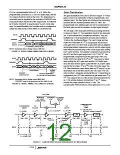
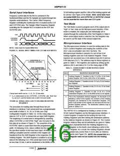
CLK
COFSYNC/
SOFSYNC
COF/
SOF
Microprocessor Interface
MSB
LSB MSB
The Microprocessor Interface is used for writing data to the
DQT’s Control Registers and reading the contents of the
AGC Loop accumulator (see AGC Section). The
NOTE: Data must be loaded MSB first.
FIGURE 21. SERIAL INPUT TIMING FOR COF AND SOF INPUTS
Microprocessor Interface consists of a set of four 8-bit
holding registers and one 8-bit Address Register. These
registers are accessed via a 3-bit address bus (A0-2) and an
8-bit data bus (C0-7). The address map for these registers is
given in Table 5. The registers are loaded by setting up the
address (A0-2) and data (C0-7) to the rising edge of WR.
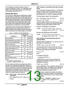
32†
30
28
26
ASSERTION OF
COFSYNC, SOFSYNC
24†
22
20
18
16†
14
12
10
8†
6
4
2
0
DATA TRANSFERED
TO HOLDING REGISTER
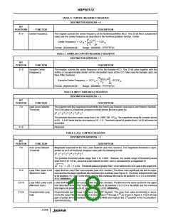
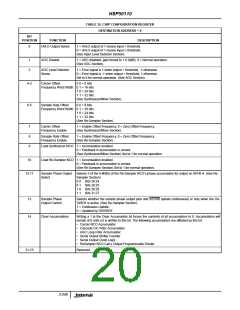
TABLE 5. ADDRESS MAP FOR MICROPROCESSOR
INTERFACE
A2-0
REGISTER DESCRIPTION
(8)
(24) (32)
(16)
0
Holding Register 0. Transfers to bits 7-0 of the 32-bit Desti-
nation Register. Bit 0 is the LSB of the 32-bit register.
1
2
3
4
Holding Register 1. Transfers to bits 15-8 of a 32-bit Destina-
tion Register.
2
6
10 14 18 22 26 30 34 38 42 46 50 54
CLK TIMES
T ††
D
T ††
D
Holding Register 2. Transfers to bits 23-16 of a 32-bit Desti-
nation Register.
T ††
D
T ††
D
Holding Register 3. Transfers to bits 31-24 of a 32-bit
Destination Register. Bit 31 is the MSB of the 32-bit register.
†Serial word width can be: 8, 16, 24, 32 bits wide.
†† T is determined by the COFSYNC, COFSYNC rate. Note that
D
This is the Destination Address Register. On the fourth CLK
following a write to this register, the contents of the Holding
Registers are transferred to the Destination Register. The
lower 4 bits written to this register are decoded into the Des-
tination Register address. The destination address map is
given in Tables 6-15.
T
can be 0, and the fastest rate is with 8-bit word width.
D
FIGURE 22. SERIAL DATA LOAD TO HOLDING REGISTERS
SEQUENCE
The procedure for loading data through these two pin
interfaces is identical. Each serial word has a programmable
word width of either 8, 16, 24, or 32 bits (see Chip
The HSP50110 is configured by loading a series of nine
32-bit Control Registers via the Microprocessor Interface. A
Control Register is loaded by first writing the four 8-bit
Holding Registers and then writing the destination address
to the Address Register as shown in Figure 23. The Control
Register Address Map and bit definitions are given in Tables
6-15. Data is transferred from the Holding Registers to a
Control Register on the fourth clock following a write to the
Address Register. As a result, the Holding Registers should
not be updated any sooner than 4 CLK’s after an Address
Register write (see Figure 23). NOTE: the unused bits in a
Control Register need not be loaded into the Holding
Register.
Configuration Register in Table 12). On the rising edge CLK,
data on COF or SOF is clocked into an Input Shift Register.
The beginning of a serial word is designated by asserting
either COFSYNC or SOFSYNC “high” one CLK prior to the
first data bit as shown in Figure 21. The assertion of the
SOFSYNC starts a count down from the programmed word
width. On following CLKs, data is shifted into the register until
the specified number of bits have been input. At this point data
shifting is disabled and the contents of the register are
transferred from the Shift Register to the respective 32-bit
Holding Register. The Shift Register is enabled to accept new
data on the following CLK. If the serial input word is defined to
be less than 32 bits, it will be transferred to the MSBs of the
3-244

 INTERSIL [ Intersil ]