HSP50110
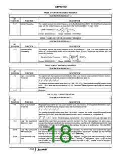
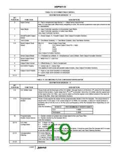
TABLE 10. I/O FORMATTING/CONTROL
DESTINATION ADDRESS = 4
BIT
POSITION
FUNCTION
Input Format
DESCRIPTION
0
1
2
0 = Two’s complement input format, 1 = Offset binary input format.
Note: if a real input with offset binary weighting is used, the unused quadrature input pins should be tied
to 1000000000.
Input Mode
0 = Input Controller operates in Interpolated Input Mode.
1 = Input Controller operates in Gated Input Mode.
(See Input Controller Section).
Serial/Parallel Output
Select
1 = Serial Output, 0 = Parallel Output. (See Output Formatter Section).
3
Test Enable
0 = Test Mode Disabled, 1 = Test Mode Enabled. (See Test Mode Section).
5-4
Serial Output Clock
Select
Bits 5-4
0 0
Serial Output Clock Rate
CLK (Serial Output Clock Pin = High)
0 1
Clk/2
1 0
1 1
CLK/4
CLK/8
(See Output Formatter Section).
6
7
Serial Output Mode
1 = I Followed by Q Mode, 0 = Simultaneous I and Q Mode. (See Output Formatter Section)
1 = MSB First, 0 = LSB First.
Serial Output Word
Orientation
8
9
Output Data Format
DATARDY Polarity
1 = Offset Binary, 0 = Two’s Complement.
1 = Active Low, 0 = Active High.
This applies to both serial and parallel output modes. (See Output Formatter Section).
10
Output Clock Polarity
1 = High to Low clock transition at midsample.
0 = Low to High clock transition at midsample.
31-11
Reserved.
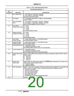
TABLE 11. DECIMATING FILTER CONFIGURATION REGISTER
DESTINATION ADDRESS = 5
BIT
POSITION
FUNCTION
DESCRIPTION
N
5-0
CIC Shifter Gain
These 6 bits set the fixed gain of the CIC shifter. The gain factor is of the form, 2 , where N is the valued
0
63
stored in this location. A gain range from 2 to 2 is provided. Since the CIC shifter sets the signal level
at the input to the CIC FIlter, care must be taken so that the signal is not shifted outside of the input bit
range of the filter. (See Gain Distribution Section).
17-6
Programmable
Divider
These 12 bits specify the divisor for the programmable divider in the Re-Sampler. The actual divisor is
equal to the 12-bit value +1 for a total range of 1 to 4096. For example, a value of 7 would produce a
sampling rate of 1/8 the CLK or 1/8 the carry-out frequency of the Re-Sampler NCO depending on con-
figuration.
(See Re-Sampler).
SOURCE
CLK
ReSampler
PROGRAMMABLE DIVIDER RANGE
1-4096
2-4096
18
Programmable
Divider Clock Source
1 = Divider clocked at sample rate of data input to the Low Pass Filter.
0 = Divider clocked by Re-Sampler NCO.
(See Re-Sampler).
20-19
CIC Filter
0 0 3 stage CIC filter.
Configuration
0 1 1 stage CIC (Integrate and dump) filter.
1 X bypass CIC.
When a 3 stage CIC filter is chosen, a decimation factor >3 must be used if the Re-Sampler NCO is used
to set the output sampling rate. (See Re-Sampler Section and Low Pass Filtering Section).
22-21
31-23
Compensation
Filtering
0 0 x/sinx filtering.
0 1 (x/sinx) filtering.
1 X bypass compensation filter.
(See Low Pass Filtering Section).
3
Reserved.
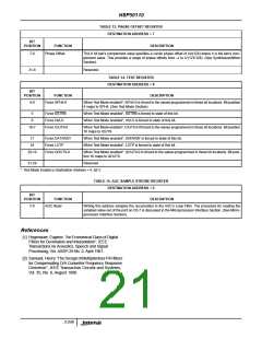
3-247

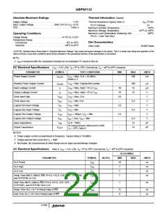
 INTERSIL [ Intersil ]