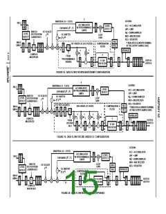
HSP50110
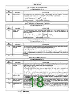
For added flexibility, the CFLD input provides an alternative
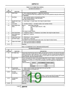
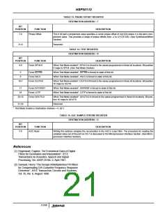
The Microprocessor Interface can be used to read the upper
8 bits of the AGC Loop Filter Accumulator. The procedure for
reading the Loop Accumulator consists of first sampling the
loop accumulator by writing 9 to the Destination Address
Register and then reading the loop accumulator value on
C0-7 by asserting RD. The sampled value is enabled for
output on C0-7 by forcing RD “low” no sooner than 6 CLK’s
after the writing the Destination Register as shown in
Figure 25. The 8-bit output corresponds to the 3 exponent
bits and 5 fractional bits to the right of the binary point (see
Figure 3). The 3 exponent bits map to C7-5 with C7 being
the most significant. The fractional bits map to C4-0 in
decreasing significance from C4 to C0.
mechanism for transferring data from the Microprocessor
Interfaces’s Holding Registers to the Center Frequency
Register. When CFLD is sampled “high” by the rising edge
of clock, the contents of the Holding Registers are
transferred to the Center Frequency Register as shown in
Figure 23. Using this loading mechanism, an update of the
Center Frequency Register can be synchronized with an
external event. Caution should be taken when using the
CFLD since the Holding Register contents will be
transferred to the Center Frequency Register whenever
CFLD is asserted. NOTE: CFLD should not be asserted
any sooner than 2 CLK’s following the last Holding
Register load. As Shown in Figure 24, the next
Configuration Register can be loaded one CLK after CFLD
has been loaded on the rising edge of CLK.
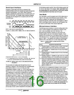
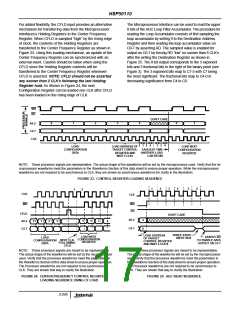
WR
RD
DON’T CARE
0
1
2
3
4
0
1
A0-2
C0-7
CLK
1
2
3
4
LOAD
CONFIGURATION
DATA
LOAD ADDRESS OF
TARGET CONTROL
REGISTER AND
WAIT 4 CLKs
LOAD NEXT
CONFIGURATION
REGISTER
EARLIEST TIME
ANOTHER LOAD
CAN BEGIN
NOTE: These processor signals are representative. The actual shape of the waveforms will be set by the microprocessor used. Verify that the mi-
croprocessor waveforms meet the parameters in the Waveforms Section of this data sheet to ensure proper operation. While the microprocessor
waveforms are not required to be synchronous to CLK, they are shown as synchronous waveforms for clarity in the illustration.
FIGURE 23. CONTROL REGISTER LOADING SEQUENCE
1
4
5
6
2
3
1
2
CLK
WR
CLK
WR
RD
CFLD
A0-2
C0-7
DON’T CARE
A0-2
C0-7
4
9
0
1
2
3
0
1
2
3
THREE-STATE
INPUT BUS
LOAD ADDRESS
OF TARGET
CONTROL REGISTER
AND WAIT 6 CLK’S
LOAD NEXT
CONFIGURATION
REGISTER
ASSERT RD
TO ENABLE DATA
OUTPUT ON C0-7
LOAD
CONFIGURATION
DATA
NEXT CLK
FOLLOWING
CFLD
NOTE: These processor signals are meant to be representative.
The actual shape of the waveforms will be set by the microprocessor
used. Verify that the processor waveforms meet the parameters in
the Waveforms Section of this data sheet to ensure proper operation.
The Processor waveforms are not required to be synchronous to
CLK. They are shown that way to clarify the illustration.
FIGURE 24. CENTER FREQUENCY CONTROL REGISTER
LOADING SEQUENCE USING CF LOAD
FIGURE 25. AGC READ SEQUENCE
3-245

 INTERSIL [ Intersil ]