BBT3821
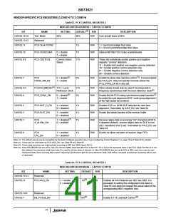
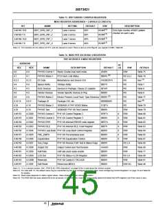
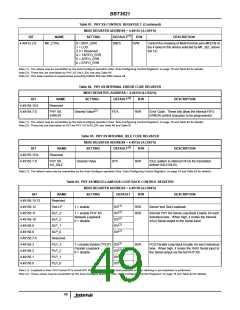
Table 73. BIST ERROR COUNTER REGISTERS
MDIO REGISTER ADDRESSES = 3.49165:6 (3.C00D:E’h)
BIT
3.49165.15:8
3.49165.7:0
3.49166.15:8
3.49166.7:0
NAME
BIST_ERR_CNT_3
BIST_ERR_CNT_2
BIST_ERR_CNT_1
BIST_ERR_CNT_0
SETTING
Lane 3 errors
Lane 2 errors
Lane 1 errors
Lane 0 errors
DEFAULT
00’h
R/W
DESCRIPTION
(1)
RCNR
Error byte counter of BIST pattern
checker on each Lane
(1)
(1)
(1)
00’h
00’h
00’h
RCNR
RCNR
RCNR
Note (1): The counters do not rollover at FF’h, and are cleared on read. There is also an error flag bit, see register 4.C007, Table 88.
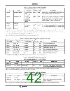
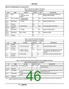
Table 74. MDIO PHY XS DEVAD 4 REGISTERS
PHY XS DEVICE 4 MDIO REGISTERS
ADDRESS
DEC HEX
4.0
AC
(2)
NAME
DESCRIPTION
DEFAULT
2040’h
R/W
R/W
DETAILS
Table 75
4.0
4.1
PHYXS Control 1 Reset, Enable loop back mode.
(3)
4.1
PHYXS Status 1
ID Code
PCS Fault, Link Status
0004’h
RO (LL)
RO
Table 76
(1)
4.2:3
4.2:3
Manufacturer and Device OUI
10Gbps Ability
01839C6V’h
0001’h
See
4.4
4.4
Speed Ability
IEEE Devices
Vendor Devices
PHYXS Status 2
Package ID
RO
Table 7
Table 8
Table 8
Table 77
4.5
4.5
Devices in Package, Clause 22 capable
Vendor Specific Devices in Pkg
001A’h
RO
4.6
4.6
0000’h
(3)
RO
4.8
4.8
Device Present, Local Fault, Type Summary 8000’h
RO
(4)
4.14:15
4.24
4.E:F
4.18
Package OUI, etc.
00000000’h
RO
See
PHYXS Status 3
PHYXS Test
10GBASE-X PHY XGXS Status
10GBASE PHY XS Test Control
1C0F’h
0000’h
0F6F’h
0800’h
00FE’h
0007’h
0000’h
0000’h
0000’h
RO
Table 78
Table 79
Table 80
Table 81
Table 82
Table 83
Table 84
Table 85
Table 87
Table 88
Table 89
Table 71
Table 90
Table 91
Table 46
4.25
4.19
R/W
R/W
R/W
R/W
R/W
R/W
R/W
R/W
RO LH
R/W
R/W
RO LH
R/W
R/W SC
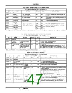
4.49152
4.49153
4.49154
4.49155
4.49156
4.49157
4.49158
4.49159
4.49160
4.49161
4.49162
4.49163
4.49167
4.C000
4.C001
4.C002
4.C003
4.C004
4.C005
4.C006
4.C007
4.C008
4.C009
4.C00A
4.C00B
4.C00F
PHYXS Control 2 PHY XS Control Register 2
PHYXS Control 3 PHY XS Control Register 3
A
A
A
A
A
A
A
PHYXS ERR
PHYXS IDLE
PHY XS Internal ERROR code register
PHY XS Internal IDLE Code Register
PHYXS Loop Back PHY XS Loop Back Control Register
PRE_EMPH
Equalization
Test_Flags
Output Ctrl
Half Rate
PHY XS Pre-emphasis level
PHY XS Equalization Control
PHY XS Receive Path Test & Status Flags 0000’h
Output Control and Test function
Half rate clock mode enable
PHY XS Status 4 LOS Register
PHY XS Control 4 TXCLK20
Reset (non MDIO)
AAAA’h
0000’h
0000’h
0000’h
0000’h
LOS Det
Reserved
Soft Reset
Note (1): ‘V’ is a version number. See “JTAG & AC-JTAG Operations” on page 53 for a note about the version number.
Note (2): For rows with “A”, the default value may be overwritten by the Auto-Configure operation (See “Auto-Configuring Control Registers” on page 16 and Table 92
for details).
Note (3): Read value depends on status signal values. Value shown indicates ‘normal’ operation.
Note (4): The IEEE 802.3ae spec allows this to be all zeroes. A XENPAK (etc.) host can more readily determine where the NVR registers are if this value is zero.
45

 INTERSIL [ Intersil ]