BBT3821
XENPAK LASI AND DOM REGISTERS (1.9000’H TO 1.9007’H & 1.A000’H TO 1.A100’H)
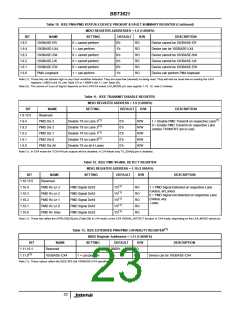
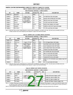
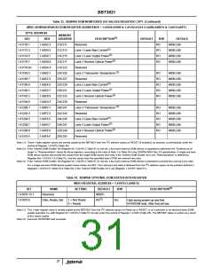
Table 24. XENPAK LASI RX_ALARM CONTROL REGISTER
MDIO REGISTER, ADDRESS = 1.36864 (1.9000’h)
(1)
BIT
1.36864.15:7
1.36864.6
1.36864.5
1.36864.4
1.36864.3
1.36864.2
1.36864.1
1.36864.0
NAME
Reserved
SETTING
DEFAULT
000’h
0’b
R/W
DESCRIPTION
PCS Byte S
RX Power
PMA LF
1 = trigger LASI by
corresponding bit of
1.36867 (1.9003’h)
0 = LASI ignores
R/W
PCS Byte Sync Fail LASI Enable
Receive Laser Pwr/Sig Det LASI Enable
PMA RX Local Fault LASI Enable
PCS RX Local Fault LASI Enable
8b/10b Code Violation LASI Enable
DOM RX or RX EFIFO Fault LASI Enable
PHY RX Local Fault LASI Enable
1’b
R/W
R/W
R/W
R/W
R/W
R/W
1’b
corresponding bit of
1.36867 (1.9003’h)
PCS LF
1’b
PCS Code
DOM RX
0’b/1’b
1’b
PHY RX LF
1’b
Note (1): Where two values are given, Default depends on LX4/CX4 select LX4_MODE pin. First value is LX4 value. The value may be overwritten by the Auto-
Configure operation (See “Auto-Configuring Control Registers” on page 16 and Table 92 for details).
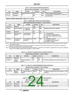
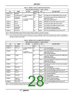
Table 25. XENPAK LASI TX_ALARM CONTROL REGISTER
MDIO REGISTER, ADDRESS = 1.36865 (1.9001’h)
(1)
BIT
1.36865.15:11
1.36865.10
1.36865.9
1.36865.8
1.36865.7
1.36865.6
1.36865.5
1.36865.4
1.36865.3
1.36865.2
1.36865.1
NAME
Reserved
SETTING
DEFAULT
R/W
DESCRIPTION
000’h
PHY S_D
LBC
1 = trigger LASI from 0’b/1’b
R/W
PHY XS Signal Detect LASI Enable
Laser Bias Current Fault LASI Enable
Laser Temperature Fault LASI Enable
Laser Output Power Fault LASI Enable
Transmit Local Fault LASI Enable
PHY XS Byte Sync Fail LASI Enable
PMA TX Local Fault LASI Enable
PCS TX Local Fault LASI Enable
Transmit EFIFO Error LASI Enable
corresponding bit of
1’b/0’b
R/W
R/W
R/W
R/W
R/W
R/W
R/W
R/W
R/W
1.36868 (1.9004’h)
0 = LASI ignores
LTEMP
LOP
1’b/0’b
1’b/0’b
1’b/0’b
0’b/1’b
1’b
corresponding bit of
1.36868 (1.9004’h)
TX LF
Byte Sync
PMA LF
PCS LF
TX EFIFO
1’b/0’b
0’b/1’b
1’b
DOM TX/
PHY Code
DOM TX or PHY XS 8b/10b Code Violation Fault LASI
Enable
1.36865.0
PHY TX LF
1’b
R/W
PHY TX Local Fault LASI Enable
Note (1): Where two values are given, Default depends on LX4/CX4 select LX4_MODE pin. First value is LX4 value. The value may be overwritten by the Auto-
Configure operation (See “Auto-Configuring Control Registers” on page 16 and Table 92 for details).
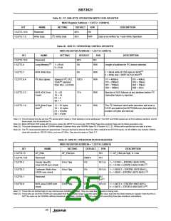
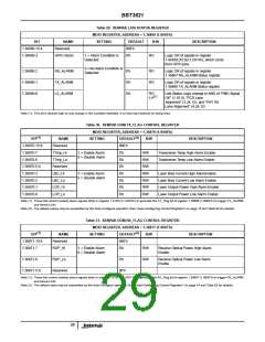
Table 26. XENPAK LASI CONTROL REGISTER
MDIO REGISTER, ADDRESS = 1.36866 (1.9002’h)
(1)
BIT
1.36866.15:4
1.36866.3
1.36866.2
1.36866.1
1.36866.0
NAME
Reserved
SETTING
DEFAULT
000’h
0’b
R/W
DESCRIPTION
(2)
GPIO
1 = trigger LASI via bit in
1.36869 (1.9005’h)
R/W
Enable GPIO pins to trigger LASI
Enable RX_Alarm to trigger LASI
Enable TX_Alarm to trigger LASI
RX_Alarm
TX_Alarm
LS_Alarm
0’b
R/W
R/W
R/W
0 = LASI ignores bit
0’b
0’b
Enable Link Status change to trigger LASI
Note (1): The default values may be overwritten by the Auto-Configure operation (See “Auto-Configuring Control Registers” on page 16 and Table 92 for details). Since
on Power up or RESET several LASI contributors will initially be in the ‘fault’ condition (in particular, Byte Synch and Lane Alignment, and their derivatives), it
may be advisable for a host to clear these before enabling these to trigger LASI.
Note (2): See description of the General Purpose Input/Output (GPIO) pins and bits for a description of how they contribute to the LASI system.
27

 INTERSIL [ Intersil ]